Pattern misalignment measurement method, program, and semiconductor device manufacturing method

Active Publication Date: 2007-10-25
TOSHIBA MEMORY CORP
View PDF18 Cites 12 Cited by
  • Summary
  • Abstract
  • Description
  • Claims
  • Application Information

AI Technical Summary

Problems solved by technology

Specifically, this has led to the following problems: 1.
The misalignment measurement in the center of a

Method used


Image

  • Pattern misalignment measurement method, program, and semiconductor device manufacturing method
  • Pattern misalignment measurement method, program, and semiconductor device manufacturing method
  • Pattern misalignment measurement method, program, and semiconductor device manufacturing method

Examples


first embodiment

(1) First Embodiment

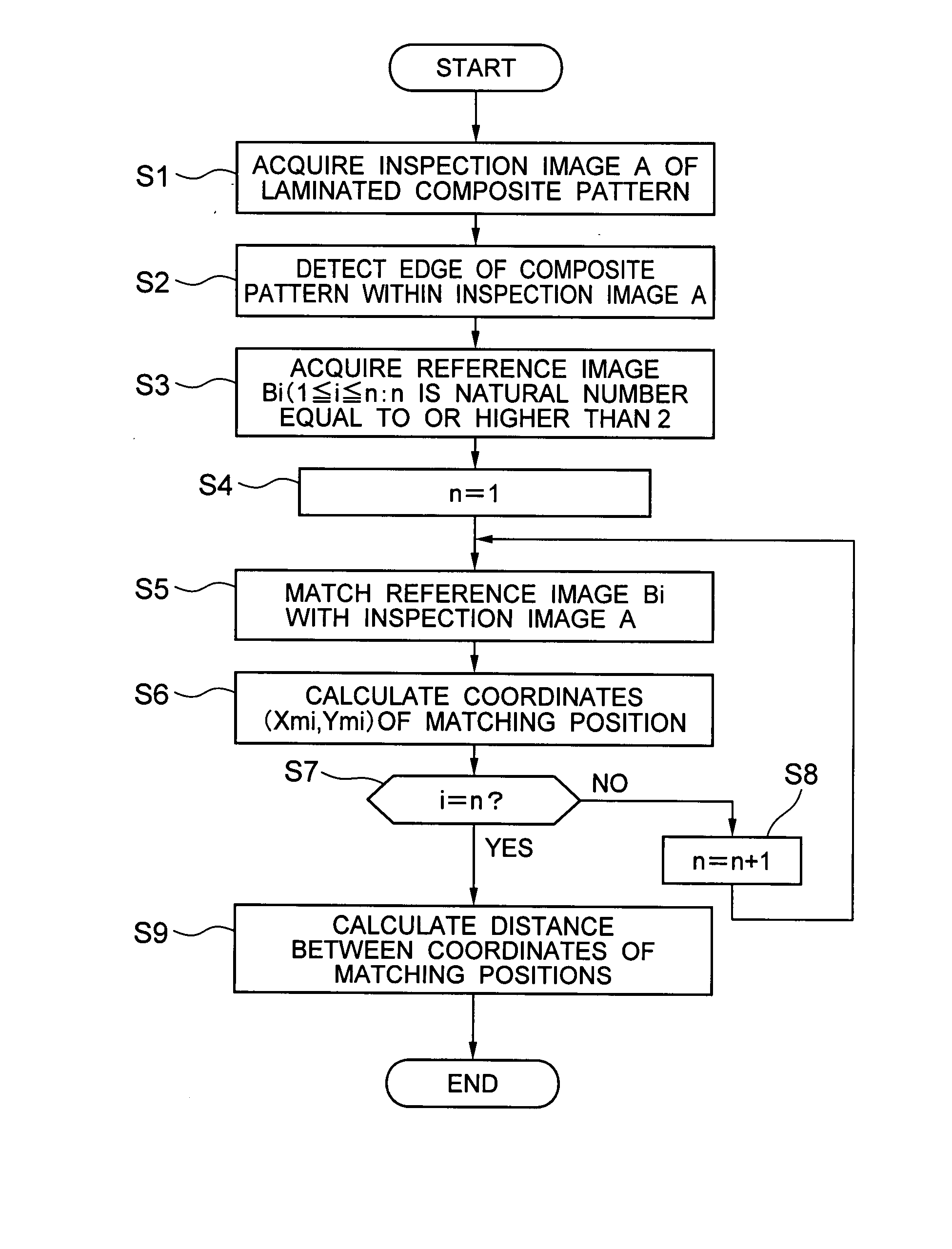
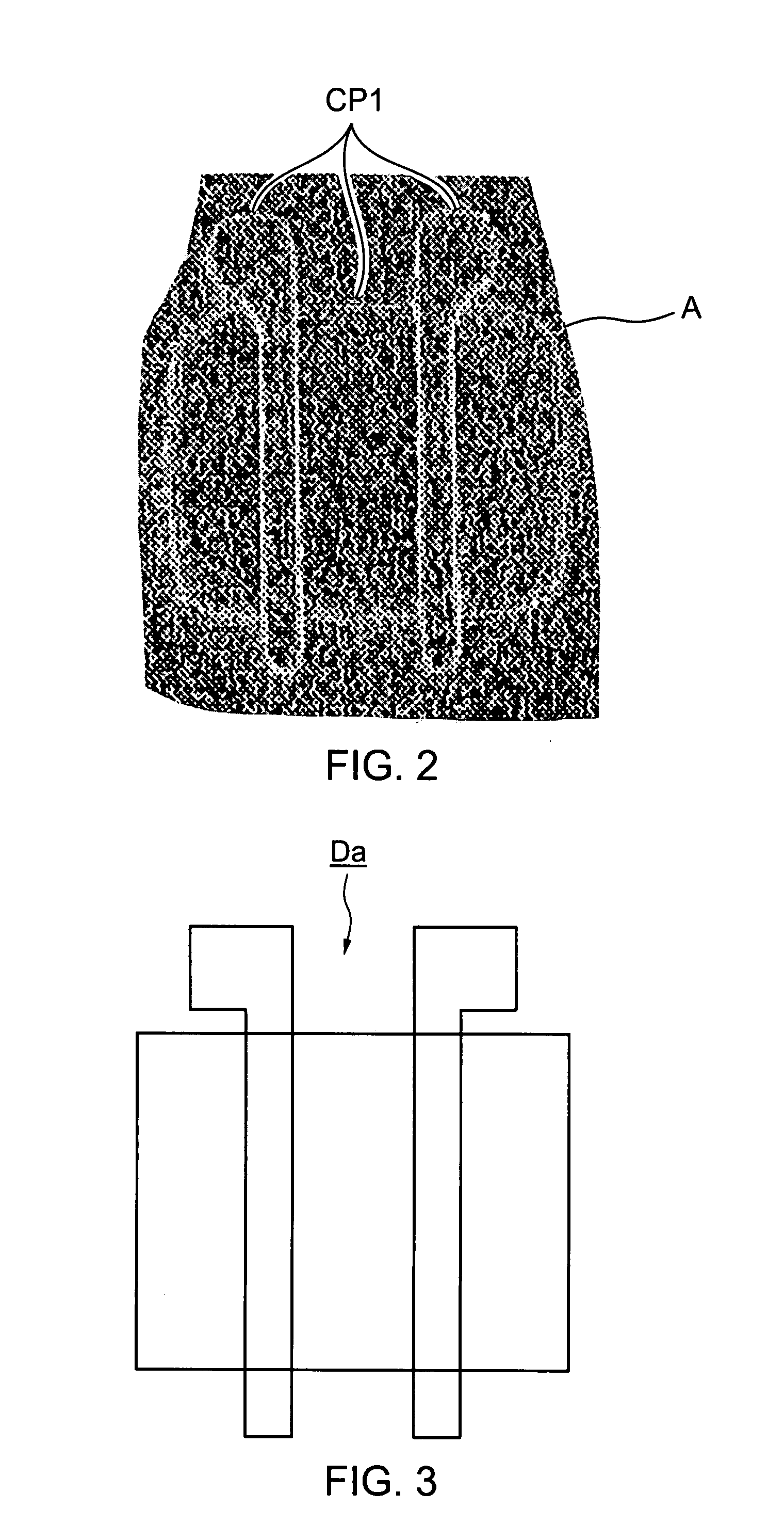
[0047] A first embodiment of the present invention will be described with reference to FIG. 1 to FIG. 9. In the present embodiment, a case will be described as an example where misalignment between single-layer patterns constituting a stack formed on a semiconductor substrate is measured using design data for the stack. The drawings except for FIG. 1 are shown in top-down view in which patterns are looked down from above. An actual pattern generally has a height in a direction vertical to the surface of the substrate. However, in a pattern measurement method of the present embodiment, misalignment is measured on the basis of an edge detected from an SEM image in the top-down view as shown in FIG. 2, so that any structure is acceptable in an actual height direction.

[0048]FIG. 1 is a flowchart showing a schematic procedure of a pattern misalignment measurement method according to the present embodiment.

[0049] First, an image A of a laminated composite pattern tar...

second embodiment

(2) Second Embodiment

[0058] A pattern misalignment measurement method according to the present embodiment enhances the accuracy of measurement by the addition of a procedure of considering the importance of an edge to the first embodiment described above.

[0059] In matching using a distance field, intrinsic values, here, values of distances from the edge of a reference pattern can be provided to edge points of an inspection image after matching processing. These intrinsic values can be allocated to, for example, 256 index colors and displayed on a display. A schematic diagram of such color display is shown in FIG. 10. In FIG. 10, portions indicated by “red” indicate that the distance from the edge is small, and the distance from the edge is greater in parts closer to portions indicated by “blue”. From such color display, it can be understood that the edges of the portions indicated by “red” are of higher importance in deciding a matching position. In addition, details of the color d...


PUM


Abstract

A pattern misalignment measurement method includes acquiring an inspection image of a composite pattern formed by superposing a plurality of kinds of element patterns on each other, acquiring reference images of at least two kinds of element patterns from reference images which are images of reference patterns of the plurality of kinds of element patterns, performing first matching of each of the acquired reference images with the inspection image, and outputting misalignment between the element patterns in the composite pattern on the basis of the result of the first matching.

Description

CROSS REFERENCE TO RELATED APPLICATION [0001] This application claims benefit of priority under 35USC §119 to Japanese patent application No. 2006-117931, filed on Apr. 21, 2006, the contents of which are incorporated by reference herein. BACKGROUND OF THE INVENTION [0002] 1. Field of the Invention [0003] The present invention relates to a pattern misalignment measurement method, a program, and a semiconductor device manufacturing method. [0004] 2. Related Background Art [0005] To take a semiconductor device as an example, an alignment technique in a photolithographic process is important in the manufacture of the semiconductor device, and a misalignment inspection process for inspecting an alignment result is an essential technique together with a critical dimension (CD) measurement process to manufacture a micro unit with a high yield. A method using an optical inspection apparatus has heretofore been used for a misalignment inspection. In addition to this method, another method h...

Claims


Application Information

Patent Timeline
IPC IPC(8): G06K9/00
CPCG06T7/001H01L21/67288H01L21/67253G06T2207/30148
Inventor MITSUI, TADASHI
Owner TOSHIBA MEMORY CORP
Why Eureka
Try Eureka