Pattern inspection apparatus, pattern inspection method, and recording medium

a pattern inspection and pattern technology, applied in the field of pattern inspection apparatus, can solve problems such as systematic failure, minute defects that cannot be recognized anywhere other than in the corners, and can not be recognized as defects, and achieve the effect of stable defect detection

Inactive Publication Date: 2005-10-13
TASMIT INC
View PDF19 Cites 60 Cited by
  • Summary
  • Abstract
  • Description
  • Claims
  • Application Information

AI Technical Summary

Benefits of technology

[0023] It is another object of the present invention to perform the matching between the pattern to-be-inspected and the reference pattern while allowing the shape difference that falls within an electrically allowable range.
[0024] Moreover, it is a still another object of the present invention to conduct stable defect detection.
[0025] Furthermore, it is another object of the present invention to enable the measurement of the two-dimensional pattern (pattern image to-be-inspected) that hitherto has been conducted on visual inspection to be executed quantitatively, rapidly and automatically.
[0048] Furthermore, the measurement of two-dimensional patterns (pattern image to-be-inspected) that hitherto have been conducted on visual inspection can be executed quantitatively, rapidly and automatically.

Problems solved by technology

The technology concerned is disclosed, for example, in the U.S. Pat. No. 5,563,702, “Automated photomask inspection apparatus and method.” However, in this technique, since a rounded part of a corner of an actual pattern formed on the wafer is likely to be recognized as a defect.
In such a circumstance where the corners are rounded, when the die to database comparative inspection is performed, it is likely that pattern deformation having no necessity of being judged as a defective corner is recognized as a defect, and this may happen frequently even with the above-described pretreatment.
Conversely, if a setting that ignores the pattern deformation of the corner is adopted, there arises a dilemma that a minute defect existing somewhere other than in the corners cannot be recognized.
Moreover, the pattern inspection on the basis of the aforesaid die-to-die comparison system cannot detect the defects that occur all over the dies on the wafer in common caused by the mask failure called the systematic failure.
That is, the same defects occur in the die to-be-inspected and in the adjacent dies that are to be compared with the die to-be-inspected, and hence the comparison between the both dies cannot lead to the detection of the defect of an individual die.
To solve the problem, although it has not been put into practical use because of calculation cost, etc., there is proposed matching inspection between the CAD data and the wafer image.
However, neither of those methods can attain an inspection speed that is usable in high-speed inspection and furthermore none of them can perform the matching while detecting the deformation quantity of the pattern.
However, unevenness of the luminance of the reference image and the like may affect recognition accuracy.
Moreover, there is a case where it is difficult to determine the inside and the outside of the pattern only from the image.
In such cases, it is often the case that it is difficult to distinguish between short circuit and deficiency and the like.
In addition, since this method cannot give information concerning which pattern is destroyed by the defect, fatal defects to the pattern and a mere defect other than such defects cannot be classified.
The inspection method using the die-to-die comparison intrinsically bears the error arising from staging precision of the inspection apparatus and precision of the optical system, and the error is approximately ten times larger than the wiring pattern width or more.
Due to this fact, even when a defect position is projected onto a pattern that the operator wishes to create (design pattern), it is impossible to specify the defect position of the pattern accurately.
It is impossible for the conventional die-to-die comparison method to inspect whether or not the OPC patterns effectively serve as corrective modification for the pattern on the wafer.
In such a case, even if the systematic defect is found at the electric inspection that is the final inspection, a quick countermeasure may not be taken to respond the short delivery time.

Method used


Image

  • Pattern inspection apparatus, pattern inspection method, and recording medium
  • Pattern inspection apparatus, pattern inspection method, and recording medium
  • Pattern inspection apparatus, pattern inspection method, and recording medium

Examples


Embodiment Construction

[0112] Hereafter, referring to the drawings, preferred embodiments of the present invention will be described in detail.

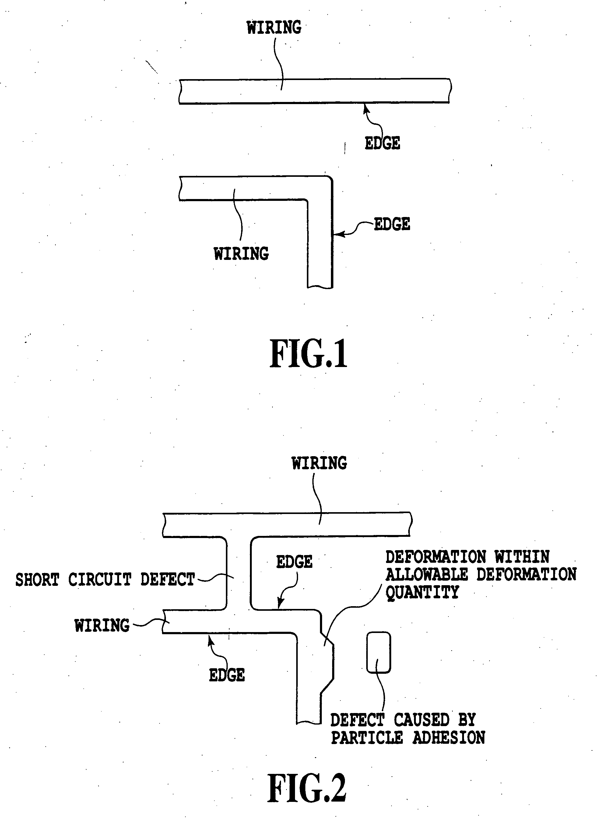
[0113]FIG. 1 is a diagram showing an example of a theoretical pattern based on the design data, and FIG. 2 is a diagram showing an example of a pattern actually manufactured based on the design data (actual pattern). As shown in FIG. 2, the actual pattern may have a short circuit defect, a defect caused by particle adhesion, and a deformation within the allowable pattern deformation quantity. Therefore, the actual pattern becomes somewhat different from the pattern theoretically obtained on the basis of the design data.

[0114] A pattern inspection apparatus according to this embodiment performs the inspection by comparing a pattern to-be-inspected (for example, the pattern shown in FIG. 2) with a reference pattern (for example, the pattern shown in FIG. 1).

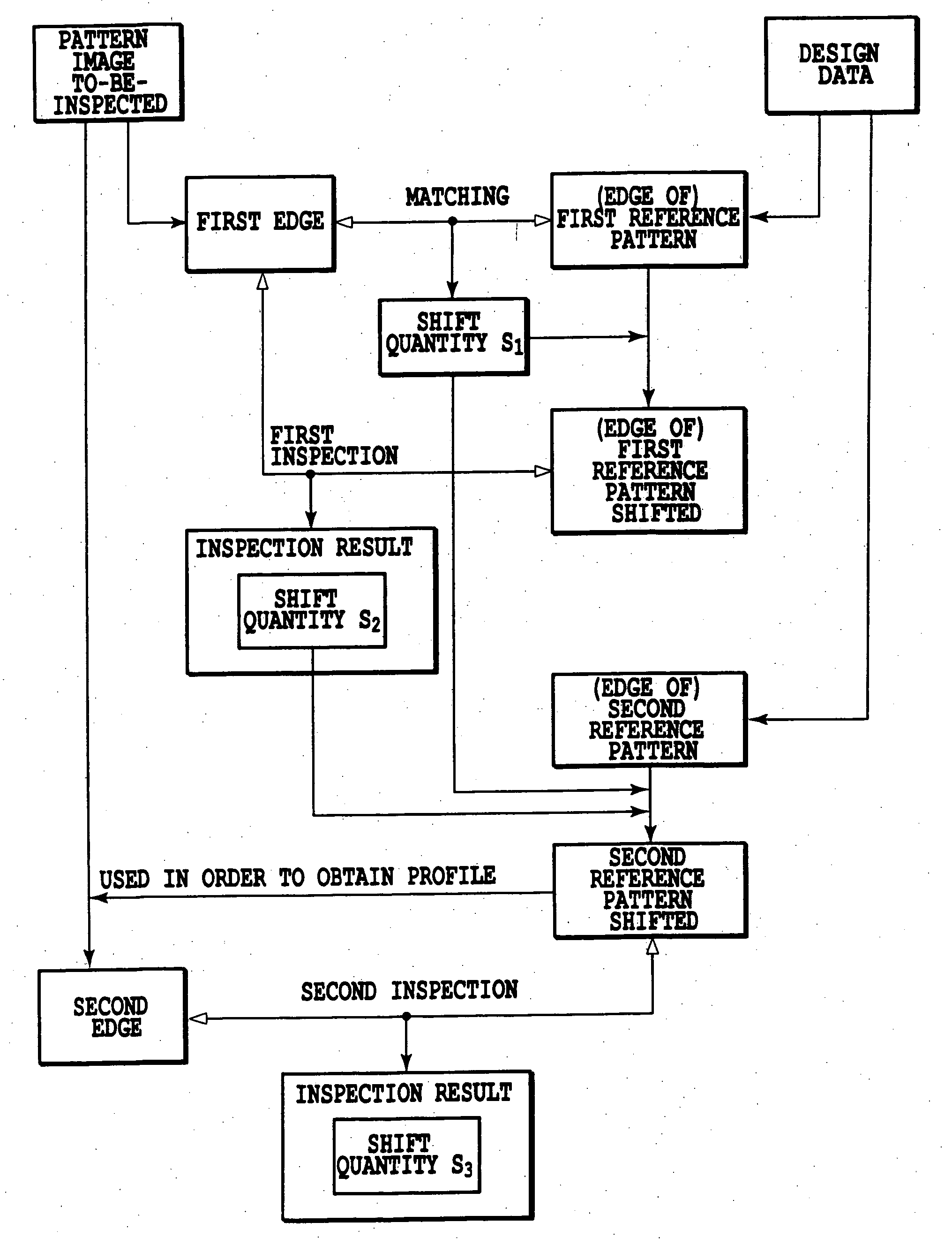
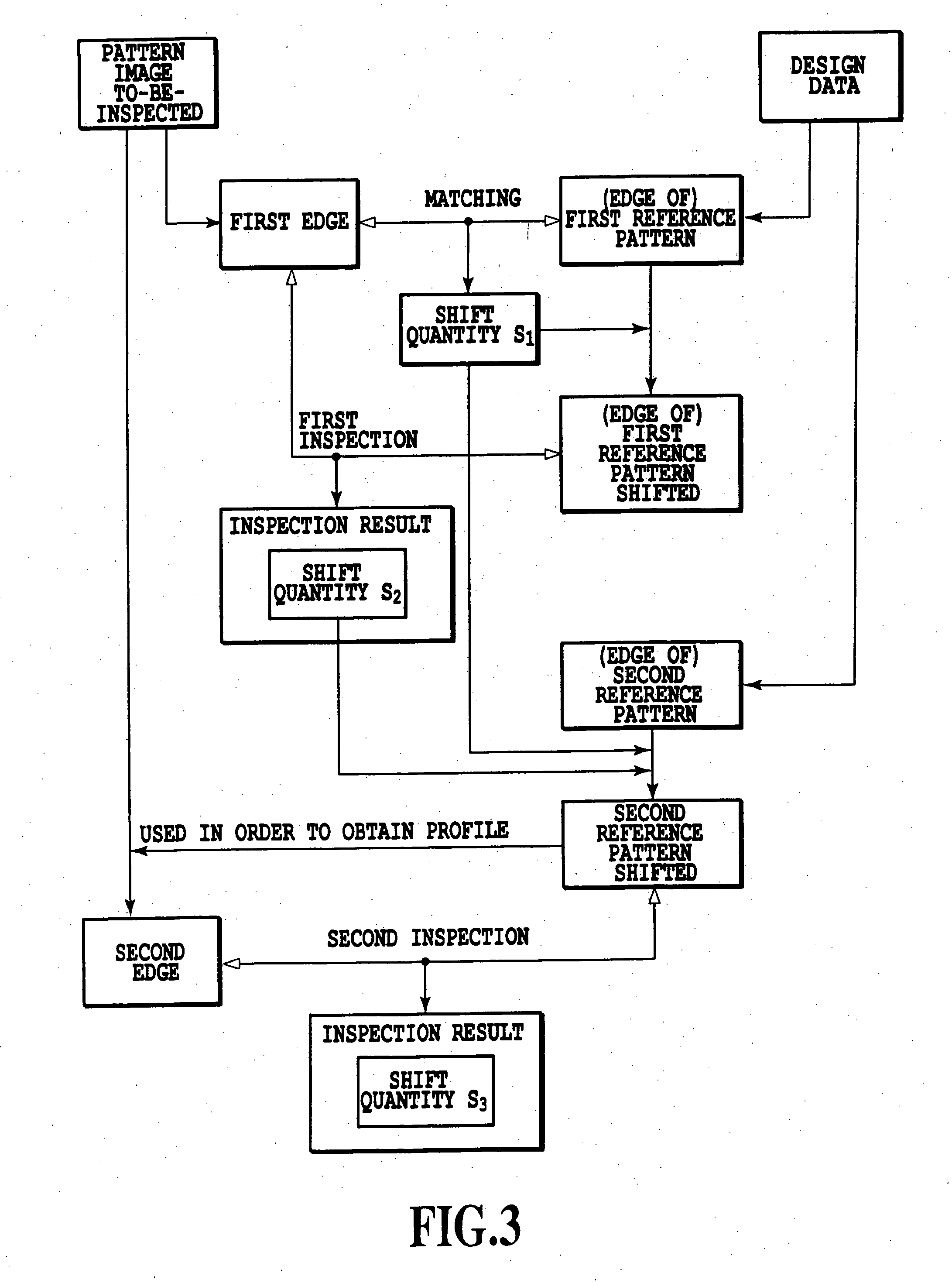
[0115]FIG. 3 is a diagram showing the outline of the inspection processing which the pattern inspection appa...


PUM

PropertyMeasurementUnit
angleaaaaaaaaaa
angleaaaaaaaaaa
distanceaaaaaaaaaa

Abstract

First, a pattern inspection apparatus detects the first edge from an image of a pattern to-be-inspected. Next, the pattern inspection apparatus conducts matching of the image of the pattern to-be-inspected and the first reference pattern by comparing the first edge and an edge of the first reference pattern. Since, as a result of the matching, a shift quantity S1 can be obtained, and then the first reference pattern is shifted by this shift quantity S1. Subsequently the pattern to-be-inspected is inspected by comparing the first edge and the edge of the first reference pattern so shifted. In this first inspection, pattern deformation quantities are obtained and defects are detected. A shift quantity S2 can be obtained as one of the pattern deformation quantities. Next, in order to detect the second edge from the pattern image to-be-inspected, the corresponding second reference pattern is shifted by a shift quantity S1+S2. Using the second reference pattern so shifted, a profile is obtained on the pattern image to-be-inspected and the second edge is detected. Then, by comparing the second edge and the edge of the second reference pattern so shifted, the pattern to-be-inspected is inspected. Also in this second inspection, the pattern deformation quantities are obtained and defects are detected. A shift quantity S3 can be obtained as one of the pattern deformation quantities.

Description

[0001] This application is based on Japanese Patent Application Nos. 11-239586 (1999) filed Aug. 26, 1999, and 2000-78847 filed Mar. 21, 2000, the contents of which are incorporated hereinto by reference. BACKGROUND OF THE INVENTION [0002] 1. Field of the Invention [0003] The present invention relates to a pattern inspection apparatus, a method for performing pattern inspection, and a recording medium. In particular, the present invention relates to a pattern inspection apparatus for inspecting fine patterns, for example, such as semiconductors (LSI), liquid crystal panels, and masks (reticles) for those, all of which are formed according to design data, to a method for performing the pattern inspection therefor, and to a recording medium therefor. [0004] 2. Description of the Related Art [0005] For the pattern inspection of wafers in the manufacturing process of semiconductor integrated circuits or the pattern inspection of masks for pattern formation thereof, an optical pattern in...

Claims


Application Information

Patent Timeline
Patent Type & Authority Applications(United States)
IPC IPC(8): G01N21/956G01N23/225G03F1/84G06K9/00G06K9/48G06T1/00G06T7/00H01L21/027
CPCG06K9/00G06K9/6206G06K2209/19G06T2207/30148G06T7/0083G06T2207/30121G06T7/001G06T7/12G06V10/754G06V2201/06G06F18/00
Inventor YAMAMOTOKITAMURA, TADASHI
Owner TASMIT INC
Why Eureka
Try Eureka