Semiconductor device and manufacturing method of same

Inactive Publication Date: 2007-11-01
KK TOSHIBA
View PDF2 Cites 8 Cited by
  • Summary
  • Abstract
  • Description
  • Claims
  • Application Information

AI Technical Summary

Problems solved by technology

According to miniaturization of a semiconductor device, a semiconductor substrate surface shape with a miniaturized active region adversely affects characteristics of the semiconductor device.
If a MOS transistor is formed in a region having such a shape, since a channel region is not flat, for example, such a problem that electric field concentrates to the end portion of the active region during programming data to the floating gate electrode 24 where a high electric field is applied and a programming characteristic dispersion occurs.

Method used


Image

  • Semiconductor device and manufacturing method of same
  • Semiconductor device and manufacturing method of same
  • Semiconductor device and manufacturing method of same

Examples


Embodiment Construction

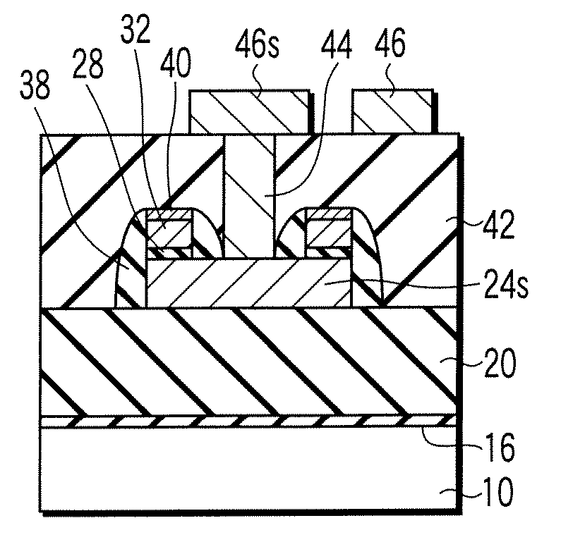
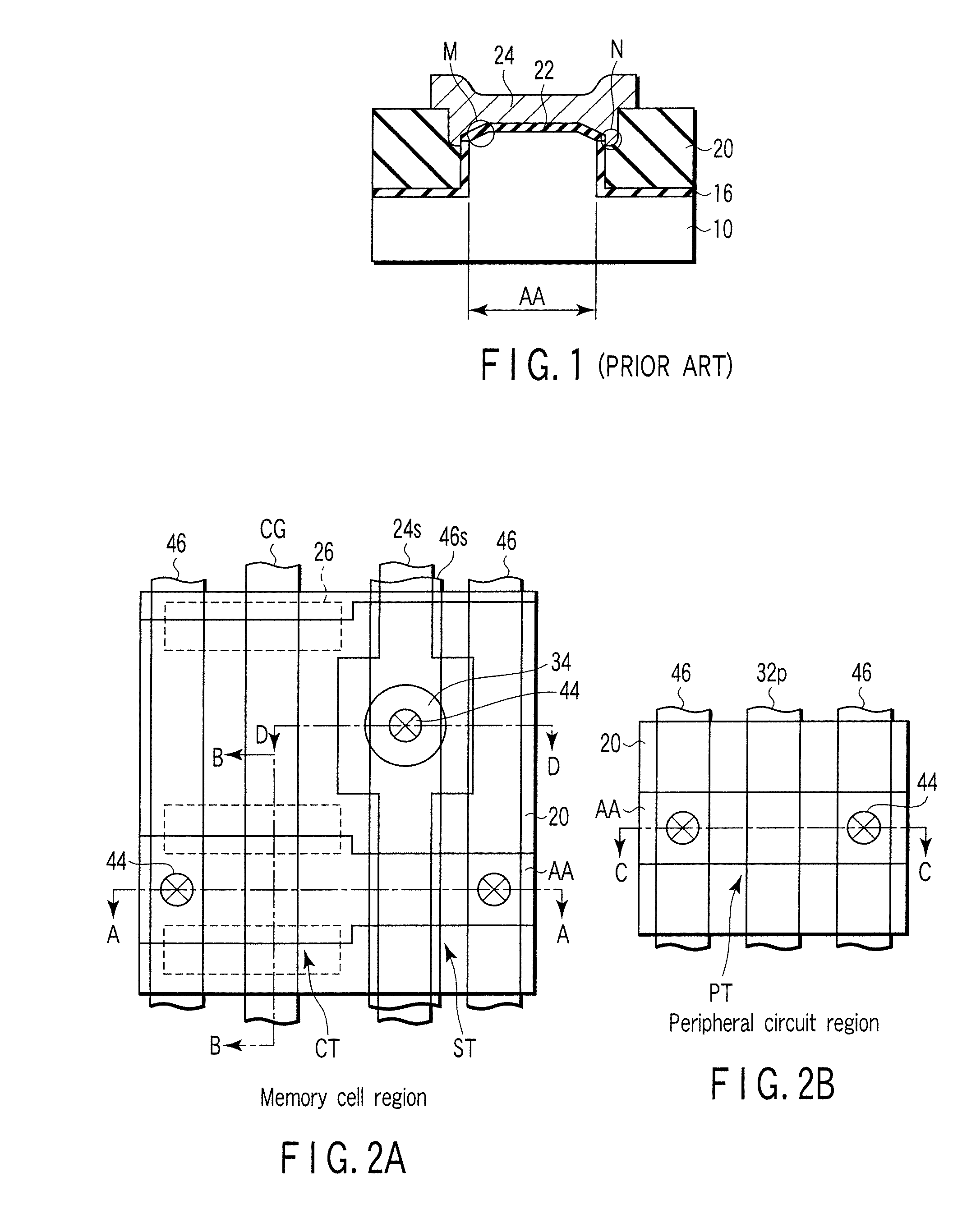
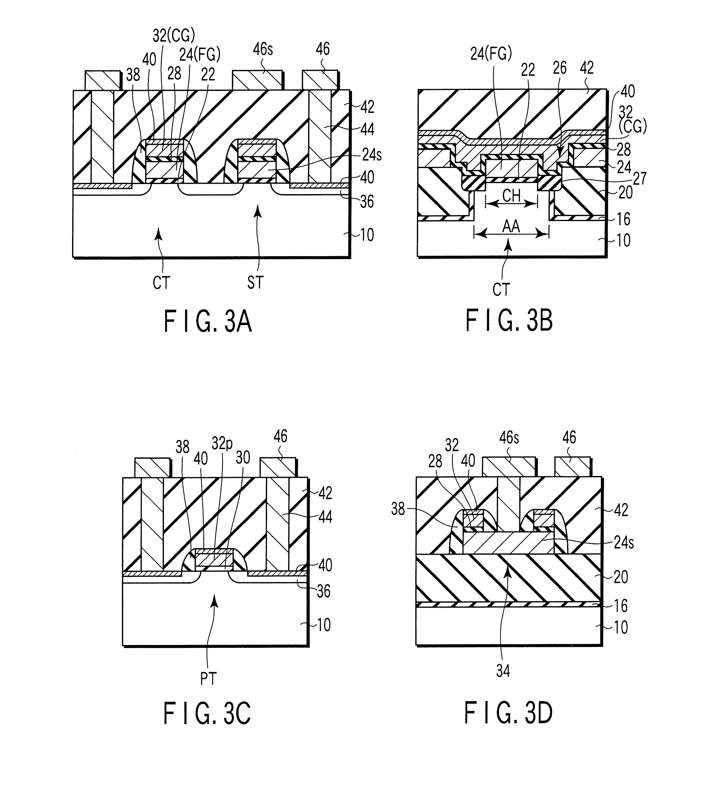
[0021]Embodiments of the present invention provide a semiconductor device in which a channel region of MOS transistor is provided not to include a non-flat active region end portion formed during a device isolation formation so as to suppress dispersion of characteristics of the semiconductor device due to a shape of the active region, and a manufacturing method thereof.

[0022]The present invention can be applied to, for example, a non-volatile storage device, such as flash memory or EEPROM, a semiconductor device embedding the non-volatile storage device and logic semiconductor device, and a manufacturing method thereof. Here, the embodiment of the present invention will be explained below in detail with regard to a semiconductor device including flash memory and peripheral circuit as an example with reference to the accompanying drawings. Throughout the drawings, corresponding portions are denoted by corresponding reference numerals. Each of the following embodiments is illustrated...


PUM


Abstract

A semiconductor device in which a channel region of MOS transistor is provided not to include a non-flat active region end portion and a manufacturing method thereof is disclosed. According to one aspect, there is provided a semiconductor device comprising a semiconductor substrate, a device isolation separating active region, wherein at least a portion of the device isolation is provided in the semiconductor substrate, and a memory cell including a memory cell transistor that comprises a channel region separated by a slit and constituted of a flat active region alone, a charge storage layer provided on a gate dielectric on the channel region, and a first gate electrode provided on an inter-electrode dielectric so as to cover the charge storage layer, and a select transistor that comprises a second gate electrode provided on the gate dielectric on the active region and electrically connected to a wiring.

Description

CROSS-REFERENCE TO RELATED APPLICATIONS[0001]This application is based upon and claims the benefit of priority from prior Japanese Patent Application No. 2006-122391, filed Apr. 26, 2006, the entire contents of which are incorporated herein by reference.BACKGROUND OF THE INVENTION[0002]1. Field of the Invention[0003]The present invention relates to a semiconductor device and a manufacturing method thereof, and in particular to a semiconductor device including a flat active region and a manufacturing method thereof.[0004]2. Description of the Related Art[0005]According to miniaturization of a semiconductor device, a semiconductor substrate surface shape with a miniaturized active region adversely affects characteristics of the semiconductor device.[0006]The active region is separated by providing device isolation, for example, shallow trench isolation (STI), to a semiconductor substrate surface. After the device isolation is formed, a mask insulator used for forming the device isolat...

Claims


Application Information

Patent Timeline
IPC IPC(8): H01L29/76
CPCH01L27/105H01L27/11536H01L27/11526H10B41/44H10B41/40
Inventor ISOBE, KAZUAKI
Owner KK TOSHIBA
Why Eureka
Try Eureka