This helps you quickly interpret patents by identifying the three key elements:
Problems solved by technology
Method used
Benefits of technology
Benefits of technology
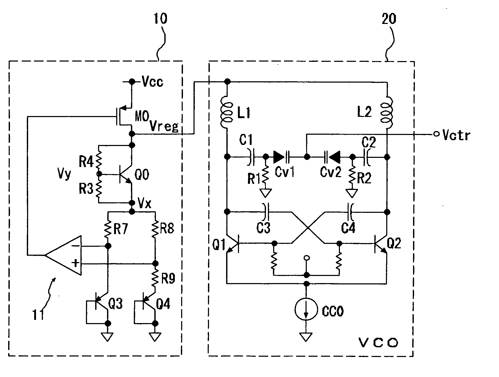
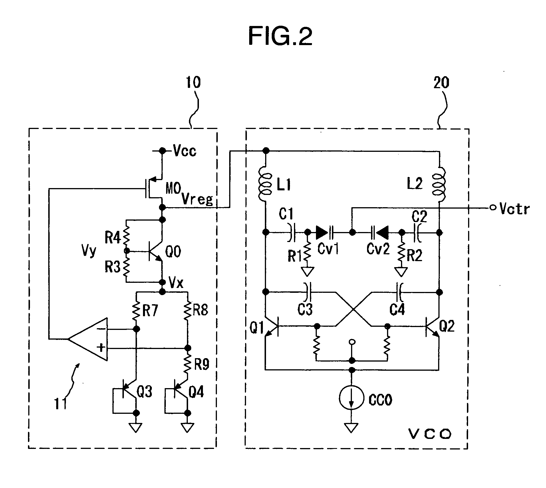
[0004] In the WCDMA radio communication system, the transmit and receive operations are performed at the same time and continuously, and therefore, as compared with the GSMpacket communication, consumes a larger amount of power and is considered to require the reduction of power consumption to secure the desired battery survival time. The oscillation circuit shown in FIG. 1 has a power supply circuit 10 for supplying a stable source voltage and therefore a lower source voltage dependency of the oscillation frequency. Nevertheless, the current consumption of the oscillation circuit is increased due to the power supply circuit 10 including the constant voltage circuit 11 and the voltage regulator 12 while at the same time posing the problem of the noise generated by the power supply circuit 10.
[0010] An object of this invention is to provide an oscillation circuit in which noises generated from the power supply circuit are minimized and a smaller amount of current is consumed while at the same time reducing the chip size.
[0014] In this circuit configuration, the band gapreference circuit and the voltage regulator can share voltage-dividing resistors (designated by R7, R8, R9 and R11, R12 in FIG. 1) and feedback differential amplifiers (AMPO, AMP1). As compared with the conventional circuit, therefore, the current consumption can be reduced remarkably while at the same time reducing the area occupied by the circuit, i.e. the chip size.
[0015] Also, the current flowing in the power supply circuit acts as an operating current for the oscillation circuit. As long as the total current remains the same as that of the circuit of FIG. 2 in which currents flow individually, therefore, the noises can be reduced by reducing the resistance value of the power supply circuit and increasing the current flowing therein. As a result, the noises can be reduced without using a bypass capacitor. At the same time, the increased package size, the increased number of parts and the resulting increased cost and the increased package area due to the addition of an external terminal can be avoided.
[0017] Specifically, according to this invention, there is provided an oscillation circuit, in which less noises are generated and a less current is consumed, while at the same time reducing the chip and package sizes and which can be suitably built in the radio-frequency IC for the mobile phones.
Problems solved by technology
In the WCDMA radio communication system, the transmit and receive operations are performed at the same time and continuously, and therefore, as compared with the GSMpacket communication, consumes a larger amount of power and is considered to require the reduction of power consumption to secure the desired battery survival time.
Nevertheless, the current consumption of the oscillation circuit is increased due to the power supply circuit 10 including the constant voltage circuit 11 and the voltage regulator 12 while at the same time posing the problem of the noise generated by the power supply circuit 10.
The noise of the power supply circuit has a serious effect on the phase noise of VCO and therefore poses a critical problem.
It is difficult, however, to embed the bypass capacitor in the IC chip due to the large capacitance thereof.
This increases the number of pins and hence the package size, resulting in an increased number of the required parts, thereby hampering the systemsize reduction.
Therefore, the use of the bypass capacitor is not a proper measure.
In proportion to reducing the resistance value, however, the current consumption is increased.
Unless the current consumption of the attached power supply circuit is also reduced as far as possible, however, the specification requirement cannot be met.
For this reason, the power supply circuit shown in FIG. 2 has proved to be still insufficient to reduce the current consumption.
Method used
Image
Click on the blue label to locate the original text in one second.
Reading with bidirectional positioning of images and text.
Examples
third embodiment
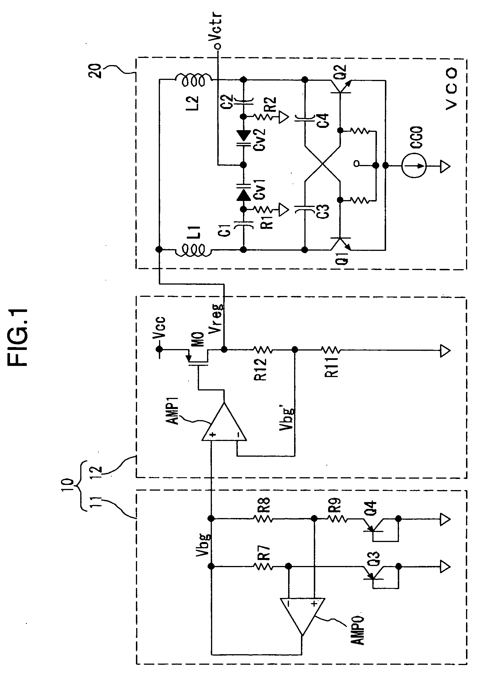
is generated. The voltage Vgs can be set arbitrarily by size adjustment of the transistors. Also, the temperature dependency of the voltage Vgs can be canceled by setting the reference voltage Vx, and by supplying the PTAT current of the band gap circuit 11 to the VCO 20, a similar effect to FIG. 3 is expected.
[0049] According to the modification shown in FIG. 6, the circuit shown in FIG. 5 is so configured that the inductors L1, L2 of the VCO are not connected in series to the transistors M1, M2 but in parallel to the varactor diodes Cv1, Cv2 between the differential output nodes with the intermediate node floating. Also, a pair of P-channel MOSFETs M3, M4 with the gate terminals and the drain terminals thereof cross-connected are connected in series to N-channel MOSFETs M1, M2 to make up a VCO of CMOS configuration. In this circuit, the regulator voltage Vreg expressed below is generated.
Vreg=Vgsn(M1)+Vgsp(M3)+Vx
[0050] The DC bias is determined by the gate-source potential Vgsn o...
second embodiment
[0051]FIG. 7 shows a power supply-integrated oscillation circuit according to the invention. In this embodiment, a VGS / R bias-type current source circuit without the transistor Q4 (M6) in series with the resistors R8, R9 is used in place of the band gap circuit as a current source circuit.
[0052] In the band gap circuit 11 according to the first embodiment, as described above, the negative temperature coefficient of the base-emitter (Vbe) of the transistor Q4 is canceled by the positive temperature coefficient of the resistors R7, R8. According to the second embodiment, on the other hand, the bias current is determined by Vgs(M5) / R9 and has a negative temperature coefficient.
first embodiment
[0053] Also, the VGS / R bias-type current source circuit according to this embodiment generates a smaller noise than the band gap circuit, and therefore, though more suitable for the low noise circuit than the first embodiment, requires another correction to secure stability against temperature. Incidentally, the transistor M5 may be a bipolar transistor instead of the MOSFET.
[0054]FIG. 8 shows a power supply-integrated oscillation circuit according to a third embodiment of the invention. Although the first and second embodiments described above use a LC resonance-type oscillator of differential configuration as a VCO. Nevertheless, the applicable VCO is not limited to such a type.
PUM
Abstract
An oscillation circuit formed in a single semiconductorchip, wherein a first source voltage is supplied to a first power supply terminal, a second sourcevoltage different from the first source voltage is supplied to a second power supply terminal, a voltage regulator receives the voltage from the first power supply terminal and outputs a source voltage, a voltage controlled oscillation circuit is supplied with a source voltage from the voltage regulator, a current source circuit is connected to the second power supply terminal, the voltage regulator, the voltage controlled oscillation circuit and the current source circuit are inserted in series between the first and second power supply terminals, and the current supplied to the voltage controlled oscillation circuit from the voltage regulator flows in the current source circuit.
Description
BACKGROUND OF THE INVENTION [0001] This invention relates to an oscillation circuit and a technique effectively applicable to a voltage controlled oscillation circuit integrated with a power supply circuit or in particular to a technique effectively applicable to a voltage controlled oscillation circuit (hereinafter referred to as the VCO) for generating a radio-frequency local oscillation signal used for down-converting a receiving signal or up-converting a transmission signal. [0002] A radio communication device such as a mobile phone uses a communication semiconductorintegrated circuit (hereinafter referred to as the radio-frequency IC) for down-converting or up-converting the frequency by combining the receiving signal or the transmission signal with a radio-frequency local oscillation signal or modulating the transmission signal or demodulating the receiving signal. A radio-frequency IC having a built-in VCO for generating a radio-frequency local oscillation signal to be combi...
Claims
Application Information
Patent Timeline
Application Date:The date an application was filed.
Publication Date:The date a patent or application was officially published.
First Publication Date:The earliest publication date of a patent with the same application number.
Issue Date:Publication date of the patent grant document.
PCT Entry Date:The Entry date of PCT National Phase.
Estimated Expiry Date:The statutory expiry date of a patent right according to the Patent Law, and it is the longest term of protection that the patent right can achieve without the termination of the patent right due to other reasons(Term extension factor has been taken into account ).
Invalid Date:Actual expiry date is based on effective date or publication date of legal transaction data of invalid patent.

