Method of hiding transparent electrodes on a transparent substrate

a transparent substrate and electrode technology, applied in the direction of instruments, conductive layers on insulating supports, transportation and packaging, etc., can solve the problems of poor screen image quality, users may not be able to input desired data or instructions successfully, etc., and achieve poor screen image quality

Active Publication Date: 2007-11-15
TRENDON TOUCH TECHNOLOGY CORPORATION
View PDF8 Cites 14 Cited by
  • Summary
  • Abstract
  • Description
  • Claims
  • Application Information

AI Technical Summary

Benefits of technology

[0016]Therefore, it is a primary objective of the present invention to provide a method of hiding transparent electrodes on a transparent substrate, and the method coats a solution of non-conductive nanoparticles onto the transparent substrate and the transparent electrodes after forming a plurality of transparent electrodes on the transparent substrate, and the reflective indexes of light for both non-conductive nanoparticles and the transparent electrodes are the same. After a high-temperature thermal processing is performed to the transparent substrate for a thermal processing time, an even mask is formed on the transparent substrate and the transparent electrodes, such that the non-conductive nanoparticles in the mask provide the same reflective index of light for the positions of the transparent substrate with and without the transparent electrodes, so as to effectively prevent a different reflective index -of light at any position of the transparent substrate that will cause a poor image quality of the screen.

Problems solved by technology

Since the reflective indexes of the two are different, the image quality of the screen observed by users will be lowered greatly, and the images of smaller graphics and texts will become blurred, and thus users may not be able to successfully press the correct buttons on the screen to execute a control instruction corresponding to the button position, and thus users may not be able to input their desired data or instruction successfully.

Method used


Image

  • Method of hiding transparent electrodes on a transparent substrate
  • Method of hiding transparent electrodes on a transparent substrate
  • Method of hiding transparent electrodes on a transparent substrate

Examples


Embodiment Construction

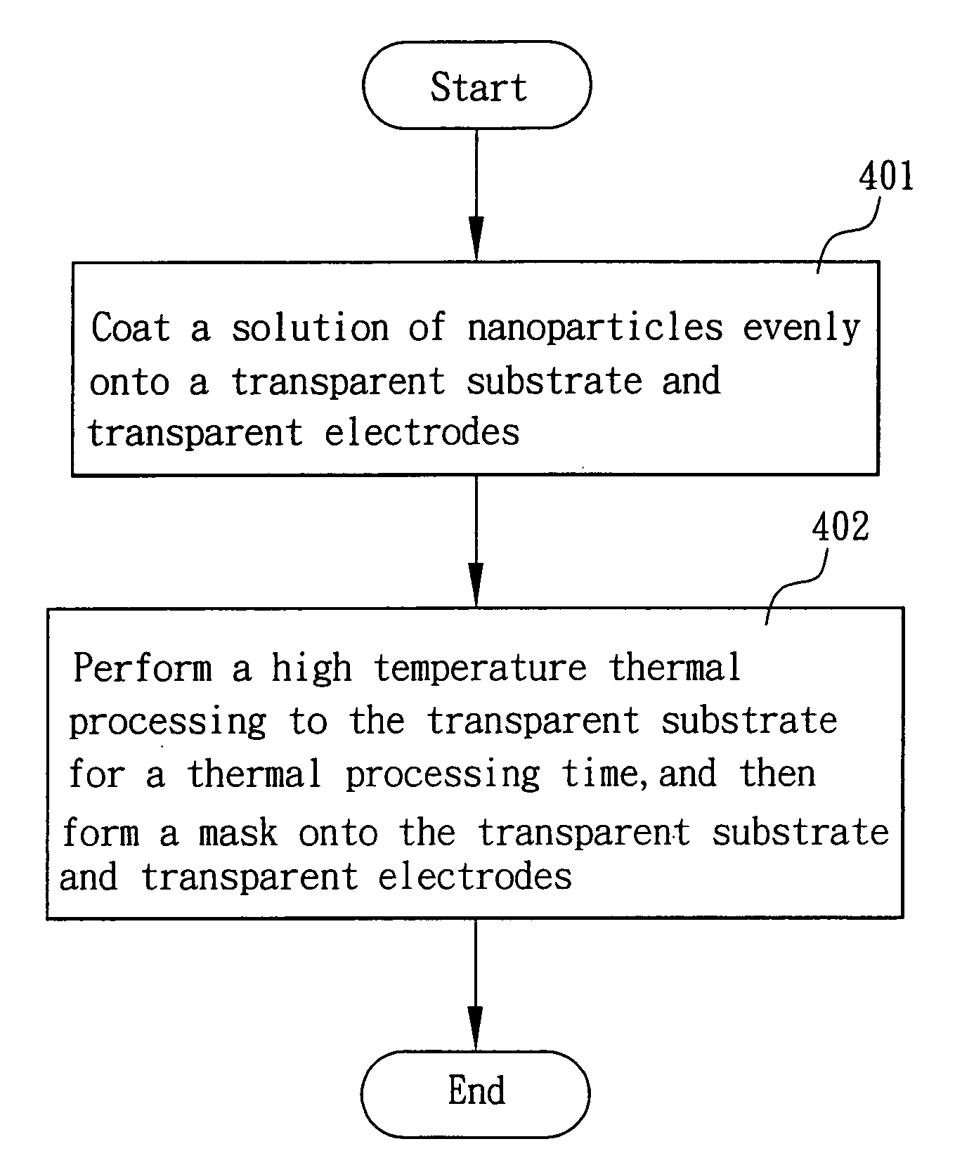
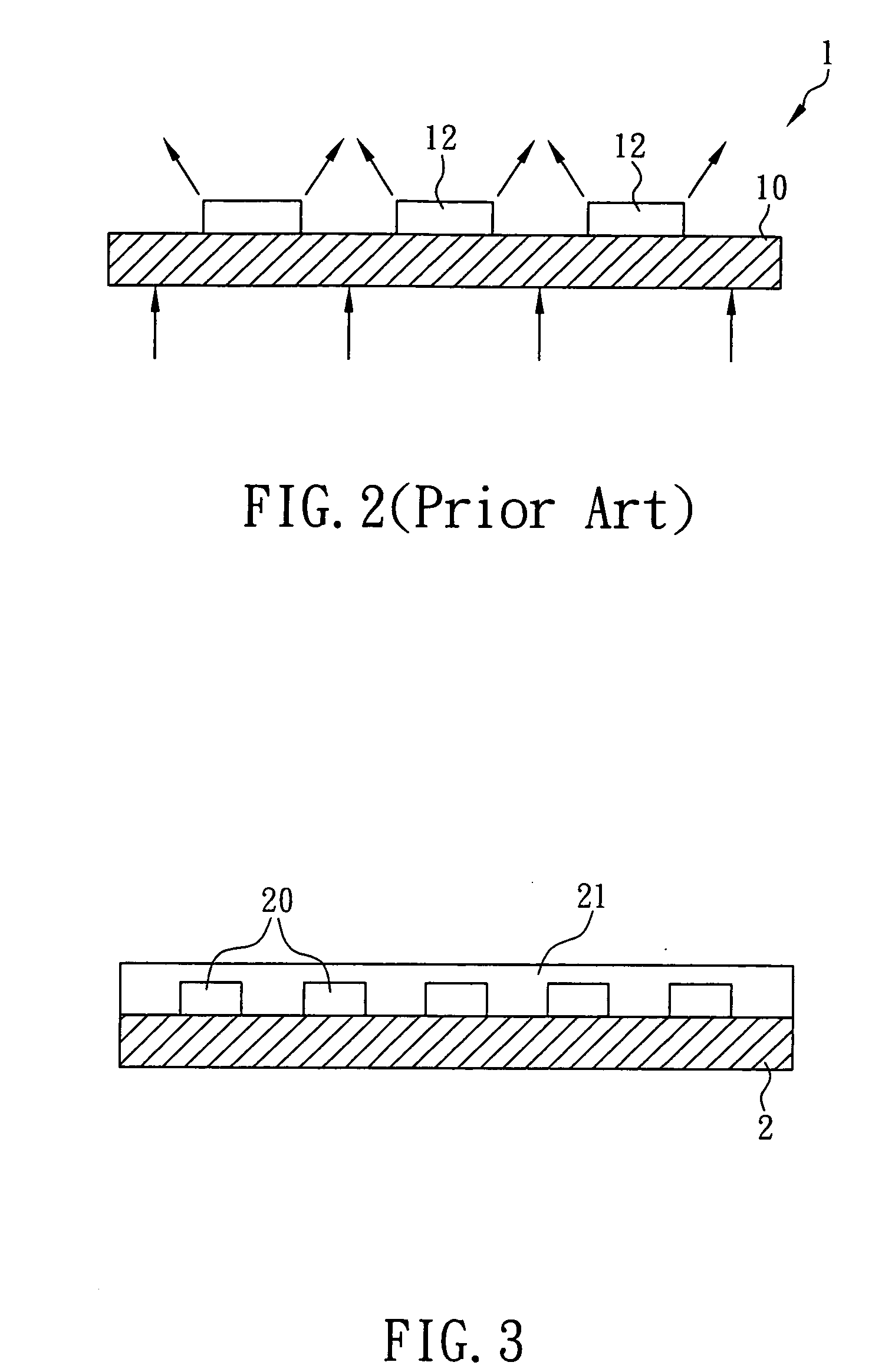
[0024]Referring to FIG. 3 for a method of hiding transparent electrodes on a transparent substrate in accordance with the present invention, the method forms a plurality of transparent electrodes 20 on a transparent substrate 2, and then coats a solution of non-conductive nanoparticles onto the transparent substrate 2 and the transparent electrodes 20. The reflective indexes of light for both non-conductive nanoparticles and transparent electrodes 20 are the same, so that the transparent substrate 2 is processed by a high-temperature thermal processing for a thermal processing time, and a flat and even mask 21 is formed on the transparent substrate 2 and the transparent electrodes 20. With the non-conductive nanoparticles in the mask 21, the reflective indexes of light at the positions of the transparent substrate 2 with or without the transparent electrodes 20 are the same, so as to effectively prevent a different reflective index of light at any position of the transparent substra...


PUM

PropertyMeasurementUnit
refractive indexaaaaaaaaaa
sizeaaaaaaaaaa
temperatureaaaaaaaaaa

Abstract

A method of hiding transparent electrodes on a transparent substrate coats a solution of non-conductive nanoparticles onto the transparent substrate and the transparent electrodes after forming a plurality of transparent electrodes on the transparent substrate, and both non-conductive nanoparticles and transparent electrodes have the same reflective index of light. After a high-temperature thermal processing is performed to the transparent substrate, an even mask is formed on the transparent substrate and the transparent electrodes, such that the non-conductive nanoparticles in the mask provide the same reflective index of light for the positions of the transparent substrate with and without the transparent electrodes, so as to effectively prevent a different reflective index of light at any position of the transparent substrate that will cause a poor image quality of the screen.

Description

FIELD OF THE INVENTION[0001]The present invention relates to a method of hiding transparent electrodes on a transparent substrate, and more particularly to a method that coats a solution of non-conductive nanoparticles onto a transparent substrate to prevent a different reflective index of light at any position of the transparent substrate that will cause a poor image quality of the screen.BACKGROUND OF THE INVENTION[0002]In recent years, technology advancement reflected to various different products, particularly the electronic, information, and communication products. These products not only come with innovative designs, structures and functions, but also meet the requirements for user-friendly application and input method as well as providing diversified features. The development of a touch panel has changed the input mode of the traditional electronic products, so that users are no longer restricted by a traditional input device (such as a press key or a mouse for inputting data...

Claims


Application Information

Patent Timeline
Patent Type & Authority Applications(United States)
IPC IPC(8): H01L21/469
CPCC03C2217/475G02F1/133502Y10T428/24926Y10T428/24802Y10T428/1064G02F1/13439C03C17/007C09K2323/051G02F1/1343G06F3/041H01B5/14
Inventor HU, CHUN-MIN
Owner TRENDON TOUCH TECHNOLOGY CORPORATION
Why Eureka
Try Eureka