
Apparatuses and methods for cleaning test probes

a technology of test probes and apparatuses, applied in the field of test probes, can solve problems such as the spin of the roller cor

Inactive Publication Date: 2007-11-22
FORMFACTOR INC
View PDF26 Cites 4 Cited by
  • Summary
  • Abstract
  • Description
  • Claims
  • Application Information

AI Technical Summary

Benefits of technology

The solution effectively removes debris from probe tips, improving electrical contact and maintaining automation in the semiconductor testing process, reducing the need for additional cleaning steps and minimizing manual intervention.

Problems solved by technology

Friction between the sticky material and the tips of the probes causes the roller core to spin as the arm moves in the horizontal direction.

Method used


Image

  • Apparatuses and methods for cleaning test probes
  • Apparatuses and methods for cleaning test probes
  • Apparatuses and methods for cleaning test probes

Examples


Embodiment Construction

[0043] The following description is of the best modes presently contemplated for practicing the invention. This description is not to be taken in a limiting sense but is made merely for the purpose of describing the general principles of the invention. The scope of the invention should be ascertained with reference to the claims. In the description of the invention that follows, like numerals or reference designators will be used to refer to like parts or elements throughout.

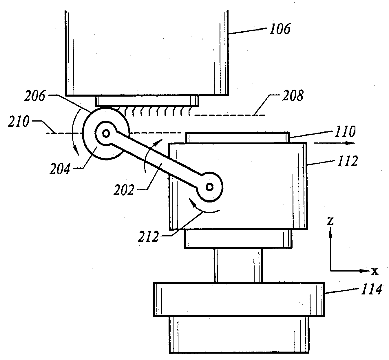
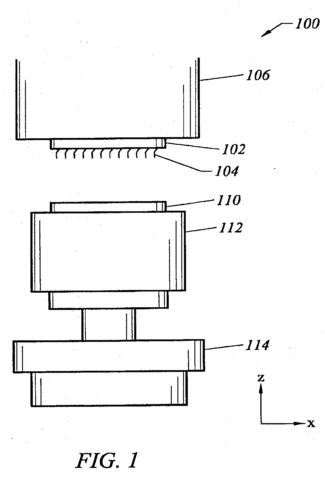
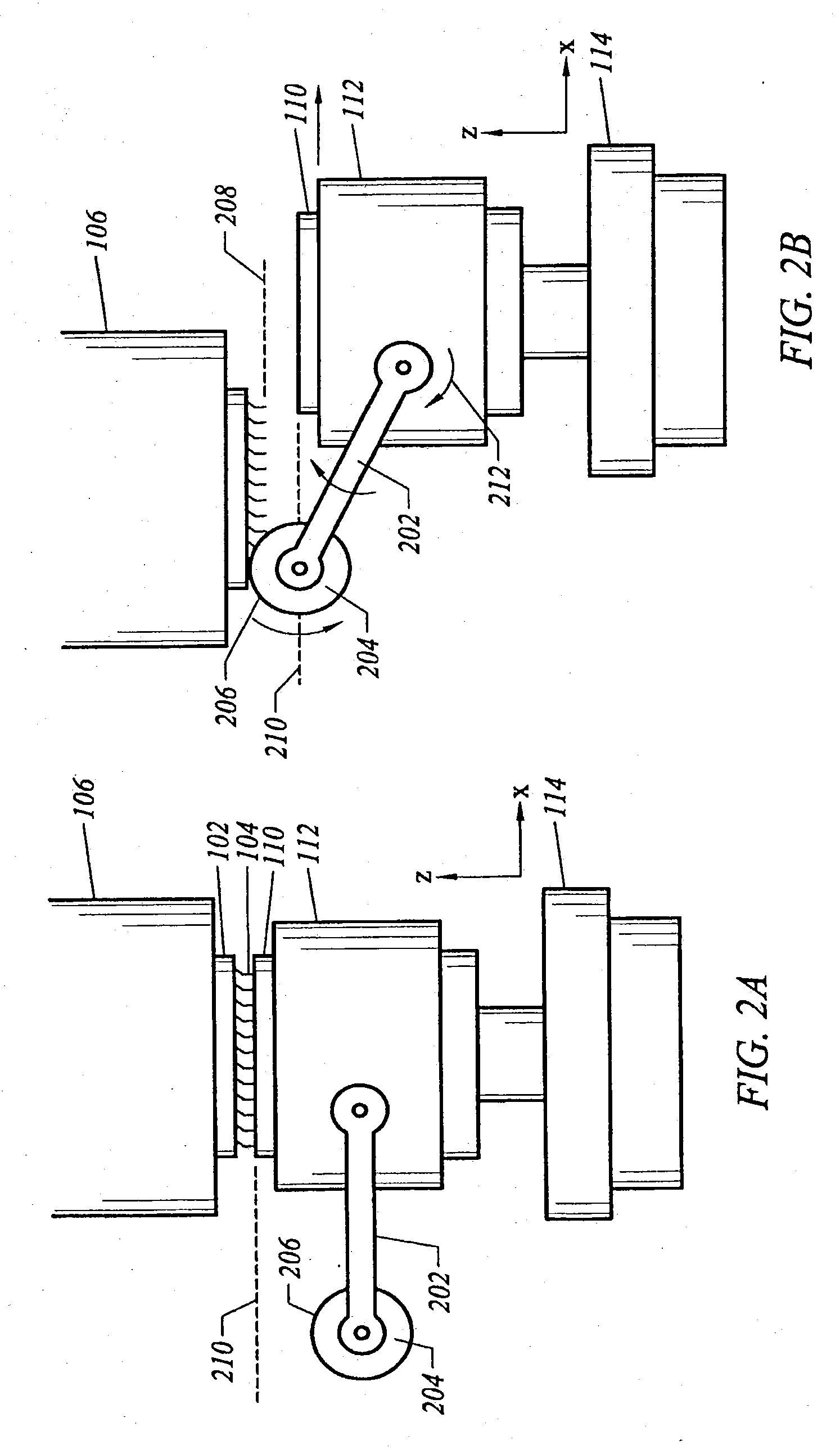
[0044]FIG. 1 is a side view of a portion of an exemplary probing-test system 100 that includes a probe card 102, a test head 106 (also known as a probe head), a wafer chuck 112, and a translation mechanism 114. One of ordinary skill in the art will appreciate that these elements have not been drawn to scale. For example, the pitch of probes elements 104 extending from probe card 102 may be such that hundreds or thousands probe elements 104 may extend from probe card 102.

[0045] A semiconductor wafer 110 is supp...


PUM


Abstract

Apparatuses and methods for cleaning test probes used in a semiconductor testing machine of the type having a plurality of test probes configured to contact the surface of a semiconductor wafer to test one or more dies formed thereon. In one embodiment, the apparatus includes a roller-support arm and a cylindrical roller supported by the roller-support arm. The roller has an outer surface comprising a sticky material. Debris on the probes will adhere to the sticky material as roller is rolled across tips of the probes. The probes are thereby cleaned.

Description

BACKGROUND OF THE INVENTION [0001] 1. Field of the Invention [0002] The present invention relates generally to probe cards that are used to perform tests on semiconductor devices. The present invention more particularly relates to the cleaning of probe elements that extend from such probe cards. [0003] 2. Background Art [0004] Individual semiconductor (integrated circuit) devices (dies) are typically produced by creating several identical dies on a semiconductor wafer, using known techniques of photolithography, deposition, and the like. Generally, these processes are intended to create a plurality of fully-functional integrated circuit devices, prior to singulating (severing) the individual dies from the semiconductor wafer. In practice, however, certain physical defects in the wafer itself and certain defects in the processing of the wafer inevitably lead to some of the dies being “good” (fully-functional) and some of the dies being “bad” (non-functional). It is generally desirabl...

Claims


Application Information

Patent Timeline
Patent Type & Authority Applications(United States)
IPC IPC(8): B08B11/00B08B7/00G01R3/00H01L21/00
CPCB08B7/0028H01L21/67028G01R3/00
Inventor GRUBE, GARY W.
Owner FORMFACTOR INC
Features
  • Generate Ideas
  • Intellectual Property
  • Life Sciences
  • Materials
  • Tech Scout
  • Unparalleled Data Quality
  • Higher Quality Content
  • 60% Fewer Hallucinations
Learn More