
Pixels and display panels

Inactive Publication Date: 2007-11-29
INNOLUX CORP
View PDF28 Cites 29 Cited by
  • Summary
  • Abstract
  • Description
  • Claims
  • Application Information

AI Technical Summary

Benefits of technology

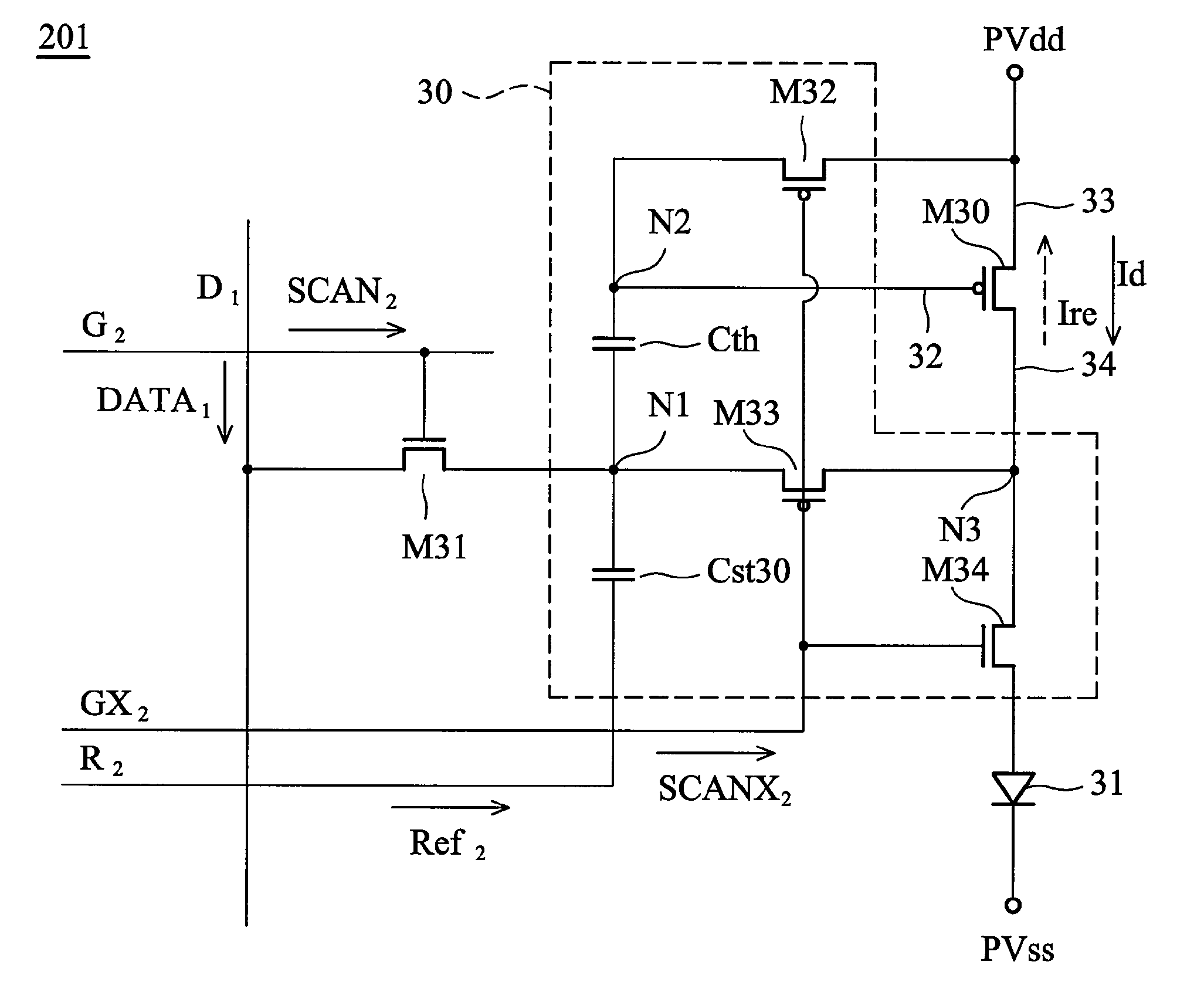
[0007]The compensation voltage can be equal to a threshold voltage of the driving transistor. Because the threshold voltage of the driving transistor is compensated by the compensation voltage, the driving transistor can generate the driving current, which is independent of the threshold voltage of the driving transistor, to drive the display device. Thus, the brightness of such a pixel can be independent of the threshold variation, and display uniformity can potentially be improved.

Problems solved by technology

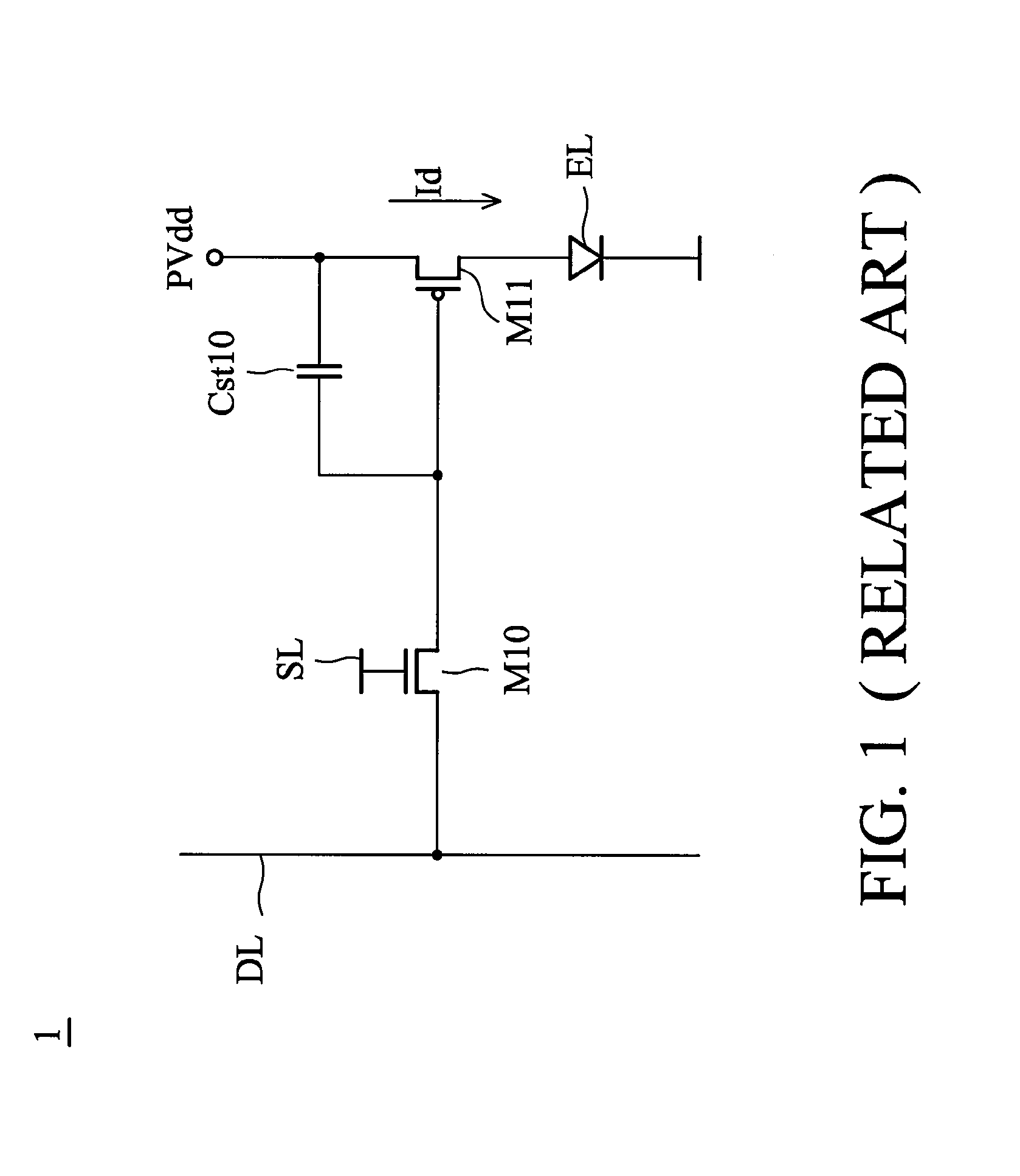
When process deviation of the driving transistor M11 occurs, threshold voltages Vth of the driving transistor M11 in the pixels are different, resulting in non-uniform brightness for pixel-to pixel and / or panel-to panel.

Method used


Image

  • Pixels and display panels
  • Pixels and display panels
  • Pixels and display panels

Examples


Embodiment Construction

[0016]The following description is of the best-contemplated mode of carrying out the invention. This description is made for the purpose of illustrating the general principles of the invention and should not be taken in a limiting sense. The scope of the invention is best determined by reference to the appended claims.

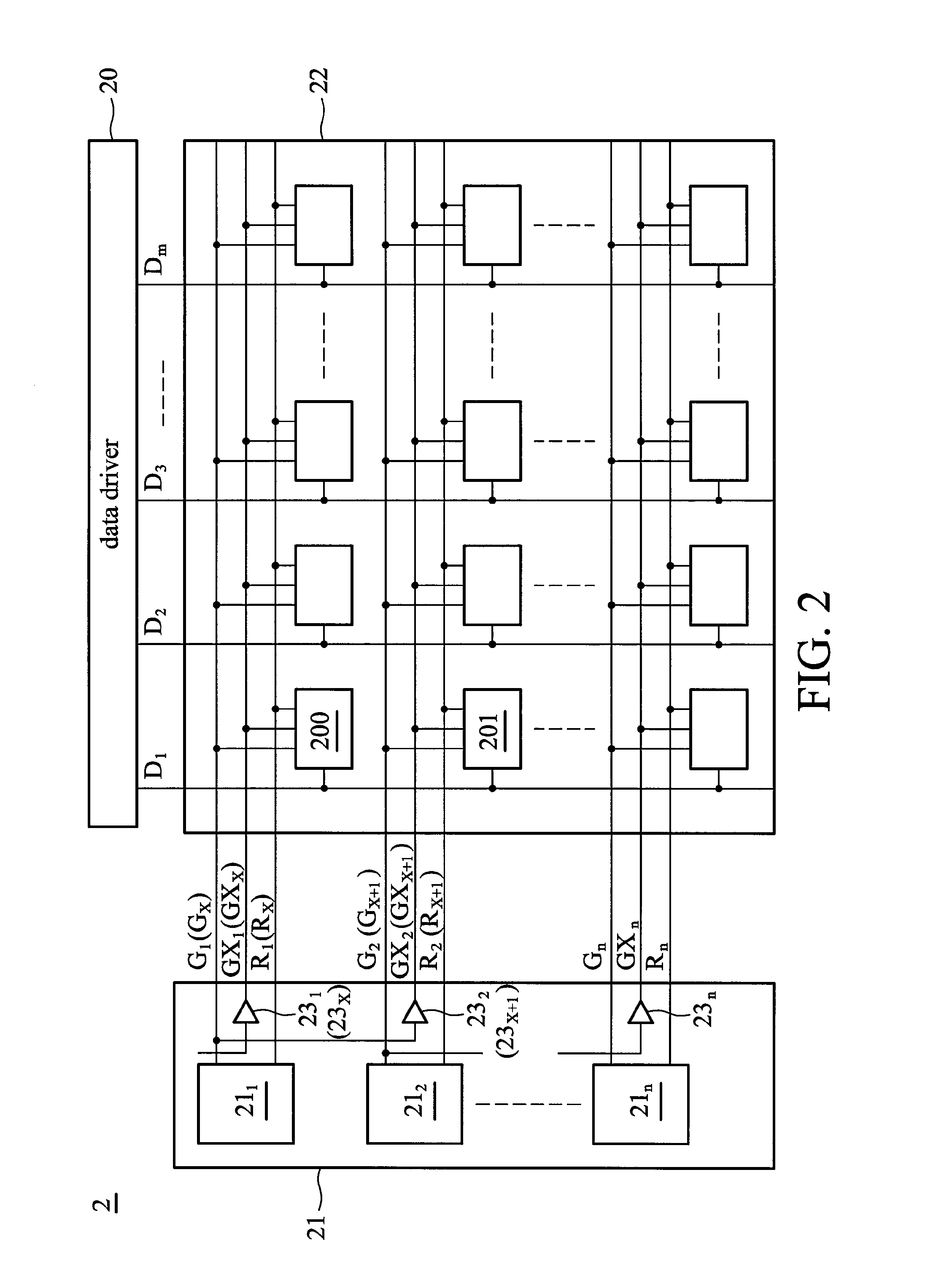
[0017]Display panels are provided. In some embodiments, as shown in FIG. 2, a display panel 2 comprises a data driver 20, a scan driver 21, and a display array 22. The data driver 20 controls a plurality of data lines D1 to Dm, and the data lines D1 to Dm respectively carry data signals DATA1 to DATAm. The scan driver 21 comprises a plurality of scan units 211 to 21n which respectively controls a plurality of scan lines G1 to Gn, and the scan lines G1 to Gn respectively carry scan signals SCAN1 to SCANn. The display array 22 is formed by intersecting data lines D1 to Dm and scan lines G1 to G1. The interlaced data line Dm and scan line Gn correspond to a display unit, ...


PUM


Abstract

A pixel providing voltage compensation and comprising a compensation device, a first switch element, a driving transistor, and a display element. The compensation device generates a compensation voltage during a first period. The first switch element transfers a data signal during a second period following the first period. The driving transistor operates in a reverse-bias mode during the first period. The driving transistor operates in a forward-bias mode during the second period to generate a driving current according to the compensation voltage and the data signal. The display element emits light according to the driving current.

Description

BACKGROUND OF THE INVENTION[0001]1. Field of the Invention[0002]The present invention relates to a pixel, and in particular relates to a display panel.[0003]2. Description of the Related Art[0004]FIG. 1 is a schematic diagram of a panel of a conventional pixel for an organic light emitting display (OLED) device. A pixel 1 comprises a switch transistor M10, a storage capacitor Cst10, a driving transistor M11, and a light-emitting diode (LED) EL. A gate of the switch transistor M10 is coupled to a scan line SL, and a drain thereof is coupled to a data line DL. When the scan line SL is asserted, it provides a scan signal SCAN to turn on the switch transistor M10. A data signal DATA on the data line DL is transmitted to a gate of the driving transistor M11, and the storage capacitor Cst10 stores the data signal DATA. According to the data signal DATA stored in the storage capacitor Cst10, the driving transistor M11 provides a driving current Id to drive the LED EL to emit light. The bri...

Claims


Application Information

Patent Timeline
IPC IPC(8): G09G3/30
CPCG09G3/3233G09G2300/0819G09G2300/0852G09G2300/0861G09G2320/043G09G2310/0254G09G2310/0262G09G2320/0233G09G2300/0876
Inventor HSIEH, MENG-HSUNPENG, DU-ZEN
Owner INNOLUX CORP
Learn More