

Voltage booster
- Summary
- Abstract
- Description
- Claims
- Application Information
AI Technical Summary
Benefits of technology
Problems solved by technology
Method used
Image

Examples
Embodiment Construction
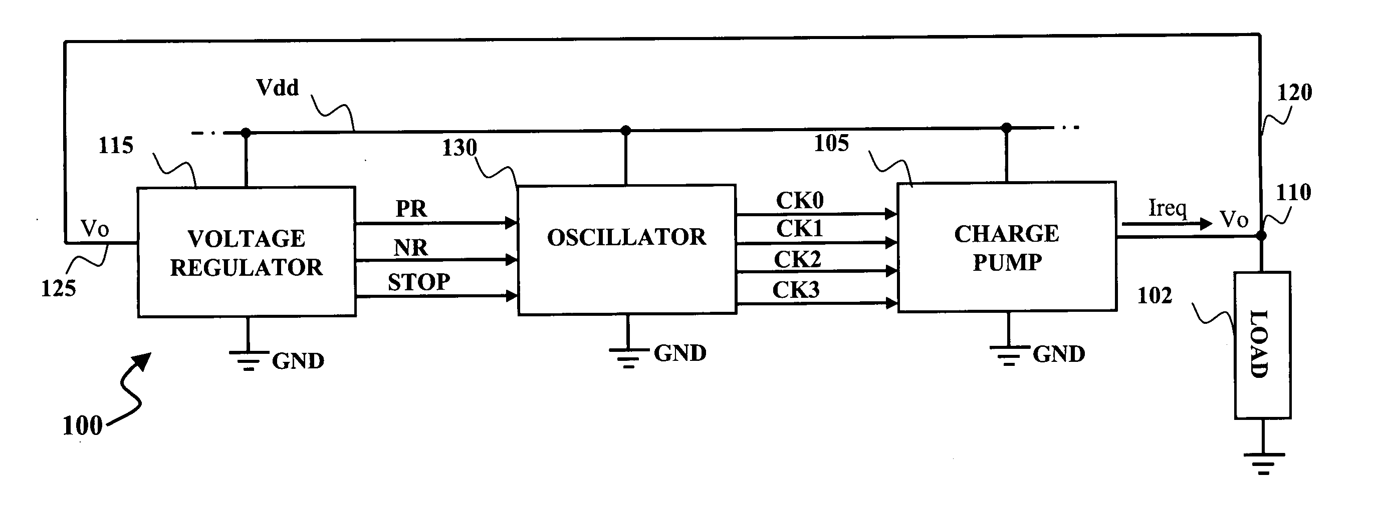
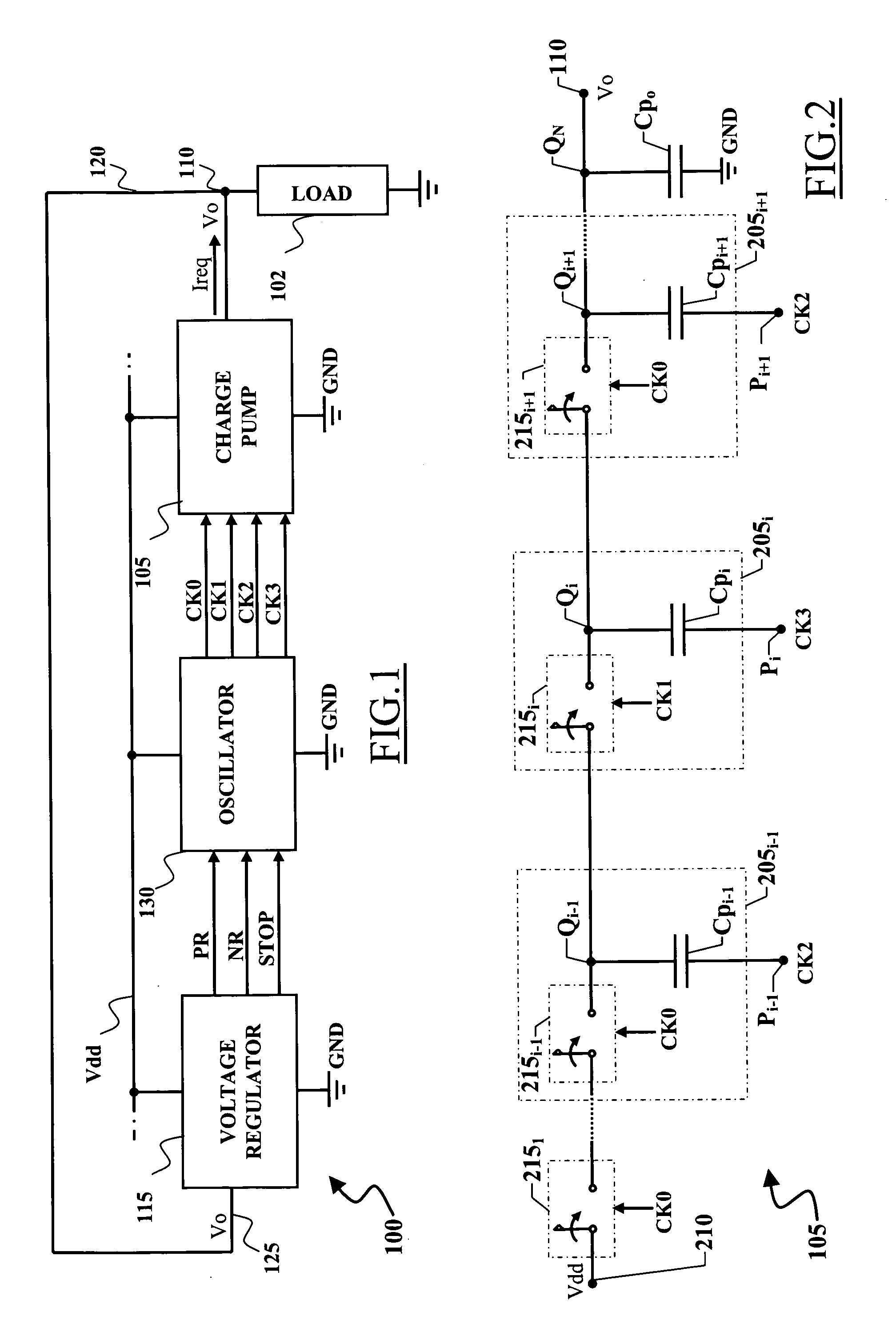
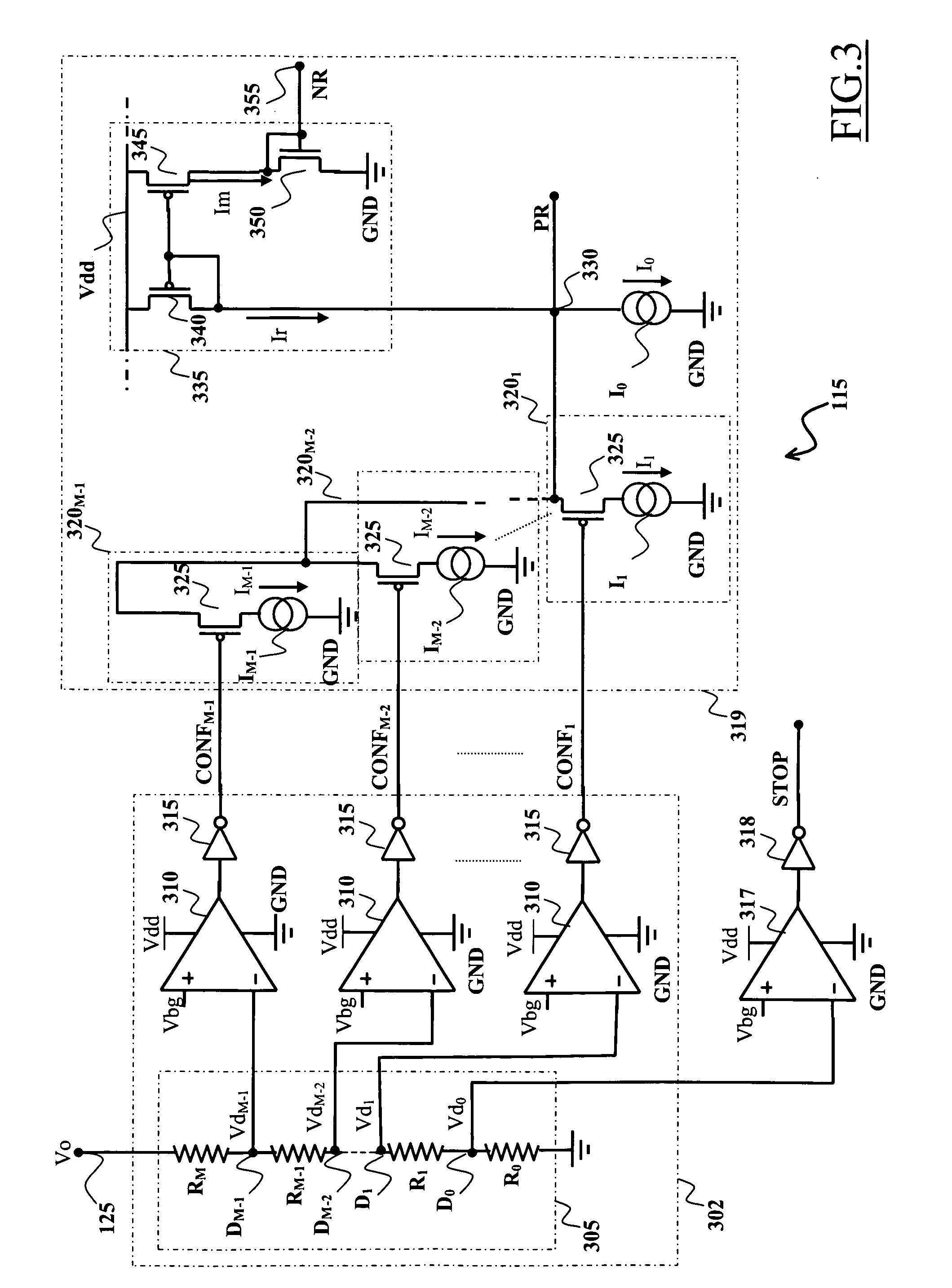
[0024]With reference to the drawings, in particular to FIG. 1, a voltage booster 100 is schematically illustrated, in terms of the functional blocks relevant to the understanding of the embodiment to be described. The voltage booster 100 is intended to be integrated in a semiconductor chip together with, for example, a flash memory (not shown in the drawing). Typically, for program and erase operations the flash memory requires an operation voltage Vo (e.g. up to 20 V) higher than a supply voltage Vdd (e.g. of 3 V) supplied to the memory from outside and distributed through a voltage supply line Vdd. In use, the voltage booster 100 generates the operation voltage Vo to be supplied, for example, to program circuits of the flash memory, acting as a circuital load 102 for the voltage booster 100 and sinking a current Ireq.
[0025]The voltage booster 100 includes a charge pump 105 adapted to generate the boosted voltage to be used as operation voltage Vo starting from the supply voltage V...
PUM
 Abstract
Description
Claims
Application Information