Eureka AIR delivers breakthrough ideas for toughest innovation challenges, trusted by R&D personnel around the world.

Appearance Inspection Apparatus

Active Publication Date: 2008-01-31
HITACHI HIGH-TECH CORP
View PDF1 Cites 11 Cited by
  • Summary
  • Abstract
  • Description
  • Claims
  • Application Information

AI Technical Summary

Benefits of technology

[0007]It is an object of the present invention to provide an appearance inspection apparatus capable of analyzing a difference in detection characteristics of detection signals obtained by a plurality of detectors, and capable of flexibly meeting various inspection purposes without changing a circuit or software.
[0014]According to the present invention, it is possible to analyze a difference in detection characteristics of detection signals obtained by a plurality of detectors on the apparatus, and capable of flexibly meeting various inspection purposes without changing a circuit or software.

Problems solved by technology

However, when it is desired to obtain an observation image of defects having different detection characteristics other than COP defects such as foreign matters adhered on the wafer surface and flaws on the wafer surface, it is necessary to recompose a signal processing circuit of a detection signal from each detector and to re-structure the software.
With this, much labor and much time are required in some cases.

Method used


Image

  • Appearance Inspection Apparatus
  • Appearance Inspection Apparatus
  • Appearance Inspection Apparatus

Examples


Embodiment Construction

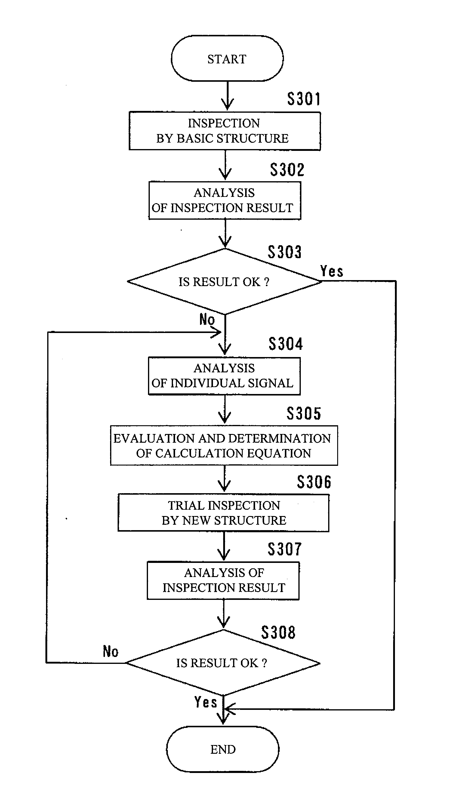
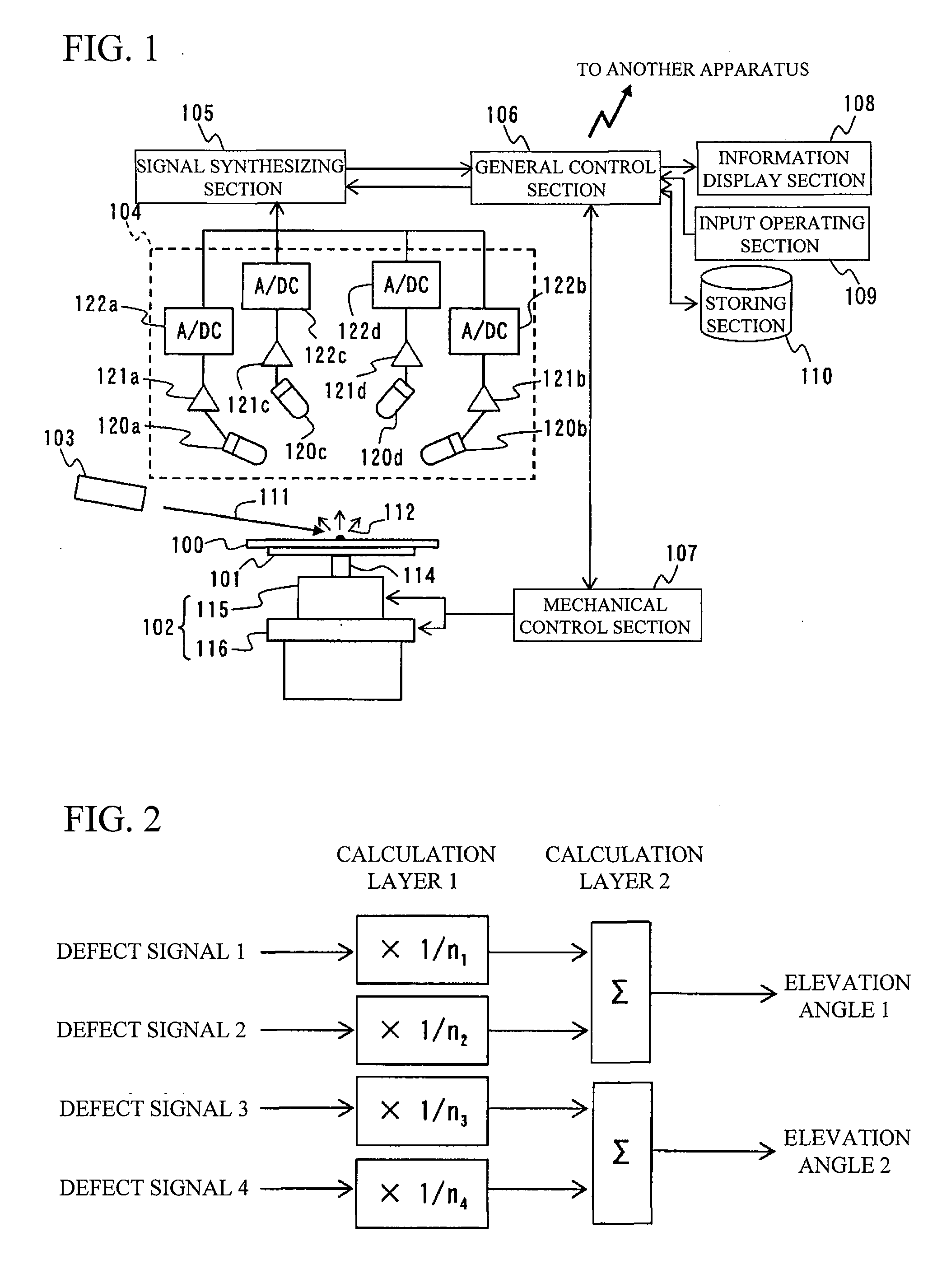
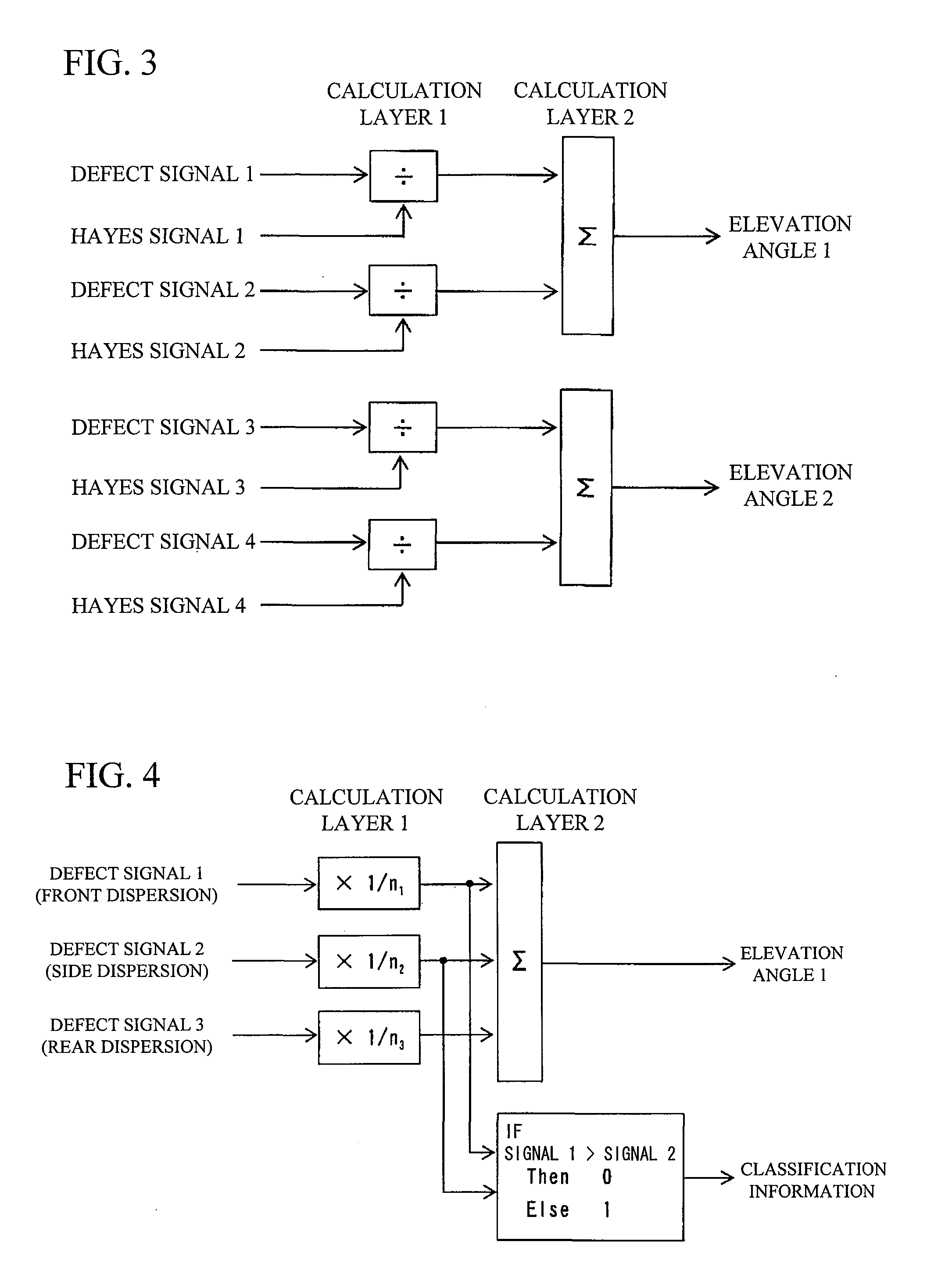
[0023]An embodiment of the present invention will be explained using the drawings below. FIG. 1 is a conceptional diagram of an appearance inspection apparatus according to the embodiment of the invention. As shown in FIG. 1, the appearance inspection apparatus includes a sample stage 101, a stage driving section 102, an illumination light source 103, a scattered light detecting section 104, a signal synthesizing section 105, a general control section 106, a mechanical control section 107, an information display section 108, an input operating section 109, a storing section 110 and the like.

[0024]The sample stage 101 supports a sample 100 of a wafer or the like placed on the sample stage 101. The stage driving section 102 drives the sample stage 101 such that a fixed point (spot) is irradiated with illumination light 111 from the illumination light source 103 and the illumination light 111 scans on the sample 100.

[0025]The stage driving section 102 includes a rotation driving sectio...


PUM


Abstract

It is an object of the present invention to provide an appearance inspection apparatus capable of analyzing a difference in detection characteristics of detection signals obtained by a plurality of detectors, and capable of flexibly meeting various inspection purposes without changing a circuit or software.An appearance inspection apparatus including a sample stage 101 for supporting a sample 100, an illumination light source 103 for irradiating the sample 100 on the sample stage 101 with illumination light 111, a plurality of detectors 120a to 120d which are disposed at different positions from each other with respect to an illumination light spot of the illumination light source 103, and which detect scattered light 112 generated from a surface of the sample 100, a signal synthesizing section 105 which synthesizes detection signals from the plurality of detectors 120a to 120d in accordance with a set condition, an input operating section 109 for setting a synthesizing condition of the detection signal by the signal synthesizing section 105, and an information display section 108 for displaying a synthesizing map 220a structured based on a synthesized signal which is synthesized by the signal synthesizing section 105 in accordance with a condition set by the input operating section 109.

Description

BACKGROUND OF THE INVENTION[0001]1. Field of the Invention[0002]The present invention relates to an appearance inspection apparatus for detecting minute foreign matters or defects on a semiconductor wafer.[0003]2. Description of the Related Art[0004]There is a technique in which in an appearance inspection apparatus for inspecting a defect on a surface of a wafer, COP (Crystal Originated Particles) defects are discriminated using a scattered light detecting section (which will appropriately be described as a multi-sensor, hereinafter) having a plurality of detectors disposed around an illumination light spot on a sample such that orientations and elevation angles thereof are different from each other, and utilizing a difference in detection characteristics caused by a difference of an elevation angle of the detectors (see Japanese Patent Application Laid-open No. 9-304289 and the like).SUMMARY OF THE INVENTION[0005]According to the technique disclosed in Japanese Patent Application ...

Claims


Application Information

Patent Timeline
IPC IPC(8): G01N21/00G06F19/00G01N21/956
CPCG01N21/8851G01N21/9501
Inventor OKA, KENJIMATSUI, SHIGERU
Owner HITACHI HIGH-TECH CORP
Why Eureka
Eureka Blog
Learn More