Growth of non-polar m-plane iii-nitride film using metalorganic chemical vapor deposition (MOCVD)

a technology of metalorganic chemical vapor deposition and m-plane iii, which is applied in the direction of crystal growth process, polycrystalline material growth, chemically reactive gas growth, etc., can solve the problems of reducing the likelihood, affecting the performance of the final device, and reducing the charge separation rate, so as to eliminate the polarization field and ensure the stability of the final devi

Active Publication Date: 2008-01-31
RGT UNIV OF CALIFORNIA +1
View PDF31 Cites 10 Cited by
  • Summary
  • Abstract
  • Description
  • Claims
  • Application Information

AI Technical Summary

Benefits of technology

[0017] The general purpose of the present invention is to grow non-polar m-plane III-nitride film using MOCVD. The method includes performing a solvent clean and acid dip of an m-SiC substrate to remove oxide from the surface of the substrate ex situ prior to growth, in situ annealing of the substrate, growing a nucleation layer on the annealed substrate, and growing the non-polar m-plane III-nitride film on the nucleation layer using MOCVD. The present invention takes advantage of non-polar nature of the m-plane III-nitride film to eliminate polarization fields, and gives rise to flexibility in growth variables, such as temperature, pressure and precursor flows, utilizing the advantage of the m-plane III-nitride film's stability during growth.

Problems solved by technology

However, as a result of c-plane growth, each material layer suffers from separation of electrons and holes to opposite faces of the layers.
Furthermore, strain at the interfaces between adjacent layers gives rise to piezoelectric polarization, causing further charge separation.
Such polarization effects decrease the likelihood of electrons and holes recombining, causing the final device to perform poorly.

Method used


Image

  • Growth of non-polar m-plane iii-nitride film using metalorganic chemical vapor deposition (MOCVD)
  • Growth of non-polar m-plane iii-nitride film using metalorganic chemical vapor deposition (MOCVD)
  • Growth of non-polar m-plane iii-nitride film using metalorganic chemical vapor deposition (MOCVD)

Examples


Embodiment Construction

[0026] In the following description of the preferred embodiment, reference is made to the accompanying drawings that form a part hereof, and in which is shown by way of illustration a specific embodiment in which the invention may be practiced. It is to be understood that other embodiments may be utilized and structural changes may be made without departing from the scope of the present invention.

[0027] Overview

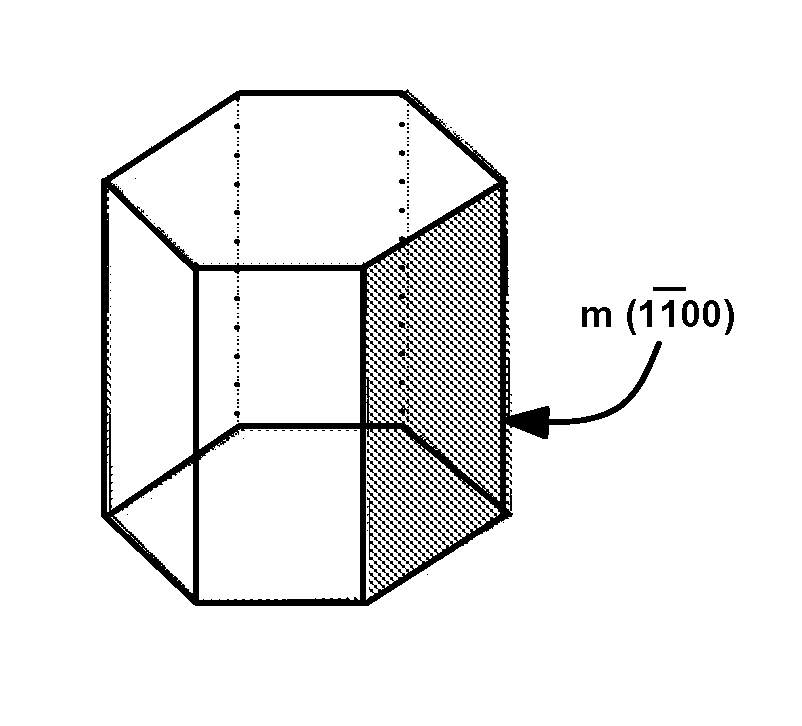
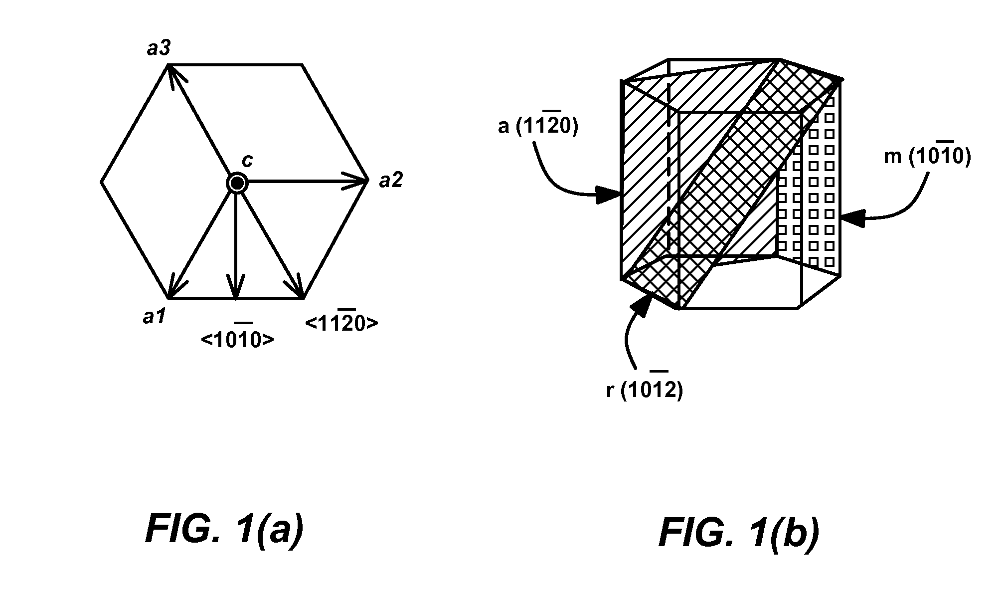
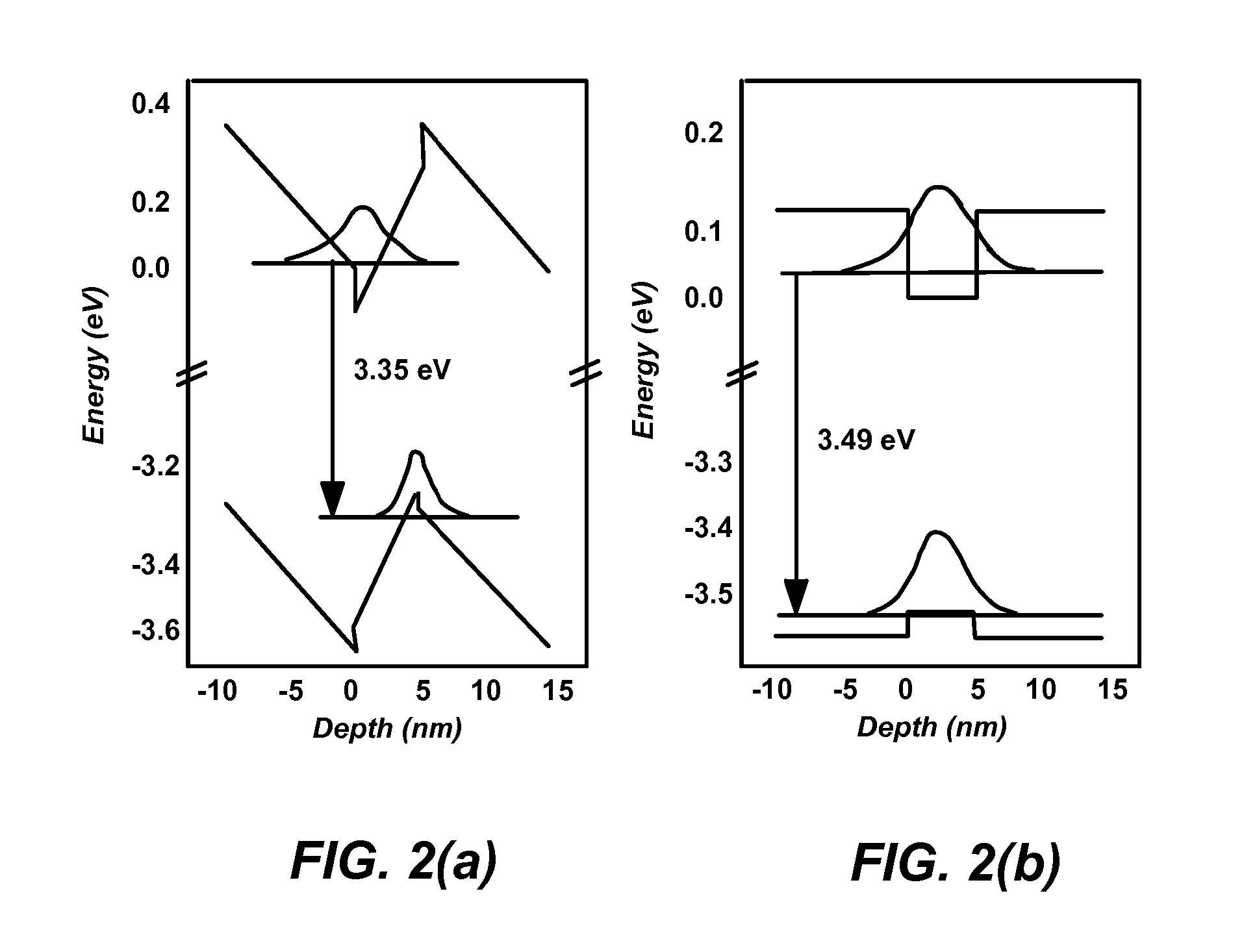
[0028] The growth of (Ga, In, Al, B)N materials in the polar [0001] c-direction causes lower performance in optical devices due to polarization fields causing charge separation along the primary conduction direction. Therefore, recent research has been conducted focusing on non-polar direction growth along a-[11-20] and m-[1-100] directions of these materials to eliminate such effects and so to improve the device performance significantly. While both a-plane and m-plane growth of GaN has been explored by HVPE and MBE, only non-polar a-{11-20} plane growth of GaN has been de...


PUM


Abstract

A method of growing non-polar m-plane III-nitride film, such as GaN, AlN, AlGaN or InGaN, wherein the non-polar m-plane III-nitride film is grown on a suitable substrate, such as an m-SiC, m-GaN, LiGaO2 or LiAlO2 substrate, using metalorganic chemical vapor deposition (MOCVD). The method includes performing a solvent clean and acid dip of the substrate to remove oxide from the surface, annealing the substrate, growing a nucleation layer, such as aluminum nitride (AlN), on the annealed substrate, and growing the non-polar m-plane III-nitride film on the nucleation layer using MOCVD.

Description

CROSS-REFERENCE TO RELATED APPLICATIONS [0001] This application is a continuation that claims the priority under 35 U.S.C. Section 120 of U.S. Utility patent application Ser. No. 11 / 444,083, filed on May 31, 2006, by Bilge M. Imer, James S. Speck and Steven P. Denbaars, entitled “GROWTH OF PLANAR NON-POLAR {1-1 0 0} M-PLANE GALLIUM NITRIDE WITH METALORGANIC CHEMICAL VAPOR DEPOSITION (MOCVD),” attorneys' docket no. 30794.136-US-U1 (2005-566), which application claims the benefit under 35 U.S.C. Section 119(e) of U.S. Provisional Patent Application Ser. No. 60 / 685,908, filed on May 31, 2005, by Bilge M. Imer, James S. Speck and Steven P. Denbaars, entitled “GROWTH OF PLANAR NON-POLAR {1-1 0 0} M-PLANE GALLIUM NITRIDE WITH METALORGANIC CHEMICAL VAPOR DEPOSITION (MOCVD),” attorneys' docket no. 30794.136-US-P1 (2005-566); both of which applications are incorporated by reference herein. [0002] This application is related to the following co-pending and commonly-assigned applications: [000...

Claims


Application Information

Patent Timeline
Patent Type & Authority Applications(United States)
IPC IPC(8): H01L21/00
CPCC30B25/02C30B25/18C30B29/403C30B29/406H01L21/02378H01L21/02389H01L21/02658H01L21/02433H01L21/02458H01L21/02516H01L21/0254H01L21/02609H01L21/0262H01L21/0242H01L21/20
Inventor IMER, BILGE M.SPECK, JAMES S.DENBAARS, STEVEN P.
Owner RGT UNIV OF CALIFORNIA
Why Eureka
Try Eureka