

Semiconductor laser diode with a ridge structure buried by a current blocking layer made of un-doped semiconductor grown at a low temperature and a method for producing the same
- Summary
- Abstract
- Description
- Claims
- Application Information
AI Technical Summary
Benefits of technology
Problems solved by technology
Method used
Image

Examples
first embodiment
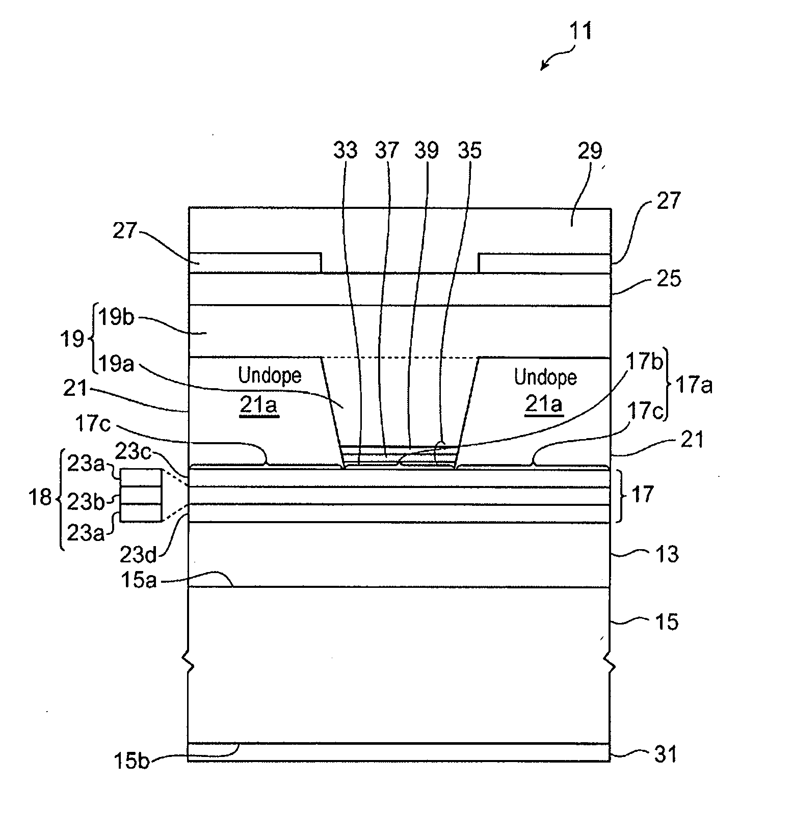
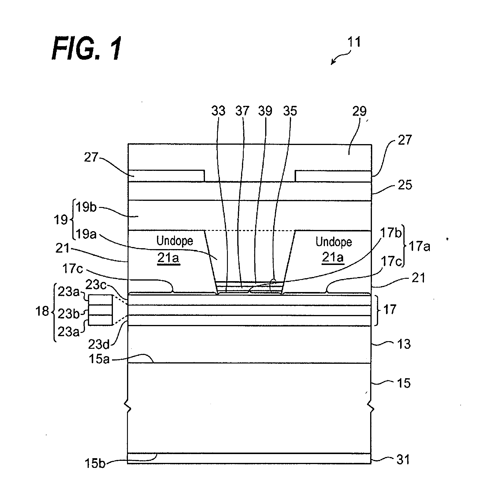
[0019]FIG. 1 is a cross section showing a semiconductor optical device according to one embodiment of the present invention. The semiconductor optical device 11 includes; a lower cladding layer 13 with the first conduction type on the primary surface 15a of the GaAs substrate 15; the active region 17, which is formed on the lower cladding layer 13, includes the first and second regions, 17b and 17c, respectively, in the primary surface 17a thereof; the upper cladding layer 19 with the second conduction type that includes a first portion 19a constituting the ridge waveguide structure on the first region 17b; and the current blocking layer 21, which is provided on the second region 17c of the active region 17 and includes a semiconductor layer 21a made of un-doped group III-V compound semiconductor material with high resistance.
[0020] In the semiconductor device 11, the current blocking layer 21 buries the first portion 19a, the ridge waveguide structure, of the upper cladding layer ...
second embodiment
[0054]FIG. 5 illustrates a semiconductor optical device according to the second embodiment of the present invention. The optical device 11c shown in FIG. 5 provides, similar to the device of the first embodiment, the lower cladding layer 13 with the first conduction type and the active region 17 on the lower cladding layer 13. These region 17 and layer 13 are provided on the GaAs substrate 15 with the first conduction type.
[0055] On the active region 17 is provided with the ridge waveguide structure 81 that includes, in addition to the upper cladding layer 83 with the second conduction type, the contact layer 85 with the second conduction type. That is, although the first embodiment provides the contact layer 25 spread in a whole region of the device, namely, on the ridge waveguide structure 19a and the current blocking layer 21a. While, the optical device according to the present embodiment comprises the contact layer 85 localized within the ridge structure 81. The current blockin...
third embodiment
[0060]FIG. 6 illustrates still another semiconductor optical device according to the third embodiment of the invention. The optical device 91 integrates a distributed feedback laser diode (hereafter denoted as DFB-LD) 91a with an optical modulator with a type of an electro-absorption (hereafter denoted as EA-modulator) 91b. The DFB-LD 91a provides the layer arrangement described previously in this specification and those materials listed in Tables may be applicable to each semiconductor layer within the device 91a.
[0061] The device 91 provides a butt-jointing structure that optically couples the DFB-LD 91a with the EA-modulator 91b. The EA-modulator 91b includes an optical absorption layer 93 which contrasts with the active layer 18 in the DFB-LD 91a and excludes the grating layer 39 and the etching-stop layer 37 underlying the grating layer 39. Except for the arrangement above, the EA-modulator 91b has layer structures and materials applied thereto substantially same as those of t...
PUM
 Abstract
Description
Claims
Application Information