Process for forming lead-free bump on electronic component

a technology of lead-free bumps and electronic components, which is applied in the direction of electrical equipment, semiconductor devices, semiconductor/solid-state device details, etc., can solve the problems of poor structural strength, reduced reliability of ag bumps, and restricted lead-contained electronic products, so as to achieve preferable mechanical strength and reliability, and increase the copper content of the solder layer

Active Publication Date: 2008-03-11
SILICONWARE PRECISION IND CO LTD
View PDF17 Cites 9 Cited by
  • Summary
  • Abstract
  • Description
  • Claims
  • Application Information

AI Technical Summary

Benefits of technology

[0011]Another objective of the invention is to provide a process for forming a copper-contained lead-free bump on an electronic component, by which a Sn—Ag—Cu bump is fabricated by reflowing a copper layer and a binary bump (such as Sn—Ag bump) without having to use a Sn—Ag—Cu solder material.
[0012]A further objective of the invention is to provide a process for forming a copper-contained lead-free bump on an electronic component, which can prevent the electronic component from warpage, delamination or cracking and provide good mechanical strength for the copper-contained lead-free bump.
[0014]Due to the property that copper ions start to diffuse at a specific range of temperature, during reflowing at a suitable reflow temperature (220-260° C.), copper ions would diffuse from the copper layer into the solder layer to thereby increase the copper content of the solder layer, making the fabricated bump have preferable mechanical strength and reliability.
[0015]Rather than using the conventional high-copper-content solder material that raises the reflow temperature profile in the prior art, the present invention separately forms the copper layer and the Sn—Ag solder material and allows copper ions to diffuse from the copper layer into the Sn—Ag solder material during reflowing so as to fabricate the Sn—Ag—Cu bump. The reflow temperature profile can be kept at 220-260° C. in the present invention using a copper-free binary Sn—Ag solder material or a ternary low-copper-content Sn—Ag—Cu solder material, unlike the solder material in the prior art having copper more than 1% that raises the reflow temperature profile to 300° C. Therefore, in the present invention, the photoresist would not be deteriorated due to over heat and can be completely removed without remaining on the chip or substrate, and also the chip or substrate can be protected against delamination, warpage or cracking caused by an extraordinarily high temperature.

Problems solved by technology

Since lead is toxic, lead-contained electronic products are becoming restricted in light of environmental protection, such that lead-free bumps are encouraged in development.
However, Sn—Ag bumps do not contain copper (Cu) and thus has poorer structural strength than Sn—Ag—Cu bumps.
During a stress reliability test in a thermal cycle, the test result shows that Sn—Ag bumps achieve lower reliability than Sn—Ag—Cu bumps, making Sn—Ag bumps less widely used than Sn—Ag—Cu bumps.
On the contrary, fabrication of Sn—Ag—Cu bumps still renders a significant drawback that is difficult to be overcome.
Accordingly, a conventional screen-printing process is usually employed to fabricate Sn—Ag—Cu bumps, in which however the content of copper would over raise a reflow temperature profile in a reflowing procedure, making the yield of the fabricated packages undesirably degraded.
Therefore, the current lead-free bump technology is still not able to produce satisfactory lead-free bumps with good reliability and feasible fabrication processes.
Sn—Ag bumps not containing copper are weaker in structural strength and achieve lower reliability in the stress reliability test as compared to Sn—Ag—Cu bumps.
For example, in the case of the copper content more than 1%, the eutectic point of the lead-free solder material is increased to about 300° C.; on the contrary, a eutectic point of Sn / Pb 63 / 37 solder material is only about 183° C. As a result, during the first reflowing procedure, an operating temperature of the Sn—Ag—Cu solder material may be increased up to 300° C., and the dry film cannot sustain such a high temperature and becomes altered or deteriorated to be difficult for complete removal.
The remaining residues of the dry film on the chip would degrade the adhesion reliability for example between an underfill material and the active surface of the chip.
Moreover, for a thermally liable material such as a laminate substrate that cannot tolerate a high temperature, the reflow temperature of 300° C. is so high to cause thermal stress generated between the chip and the substrate, which may lead to problems such as deformation or delamination of the chip and the substrate, deterioration of the electrical performance and cracking of the chip, and degradation of the yield.
Therefore, the problem to be solved here is to provide a process for forming a copper-contained lead-free bump on an electronic component under an appropriate reflow temperature profile.

Method used


Image

  • Process for forming lead-free bump on electronic component
  • Process for forming lead-free bump on electronic component
  • Process for forming lead-free bump on electronic component

Examples


first preferred embodiment

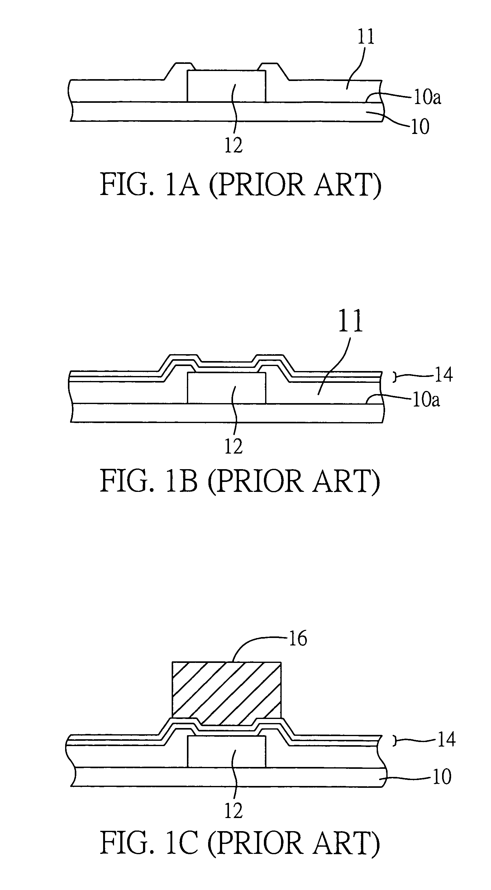
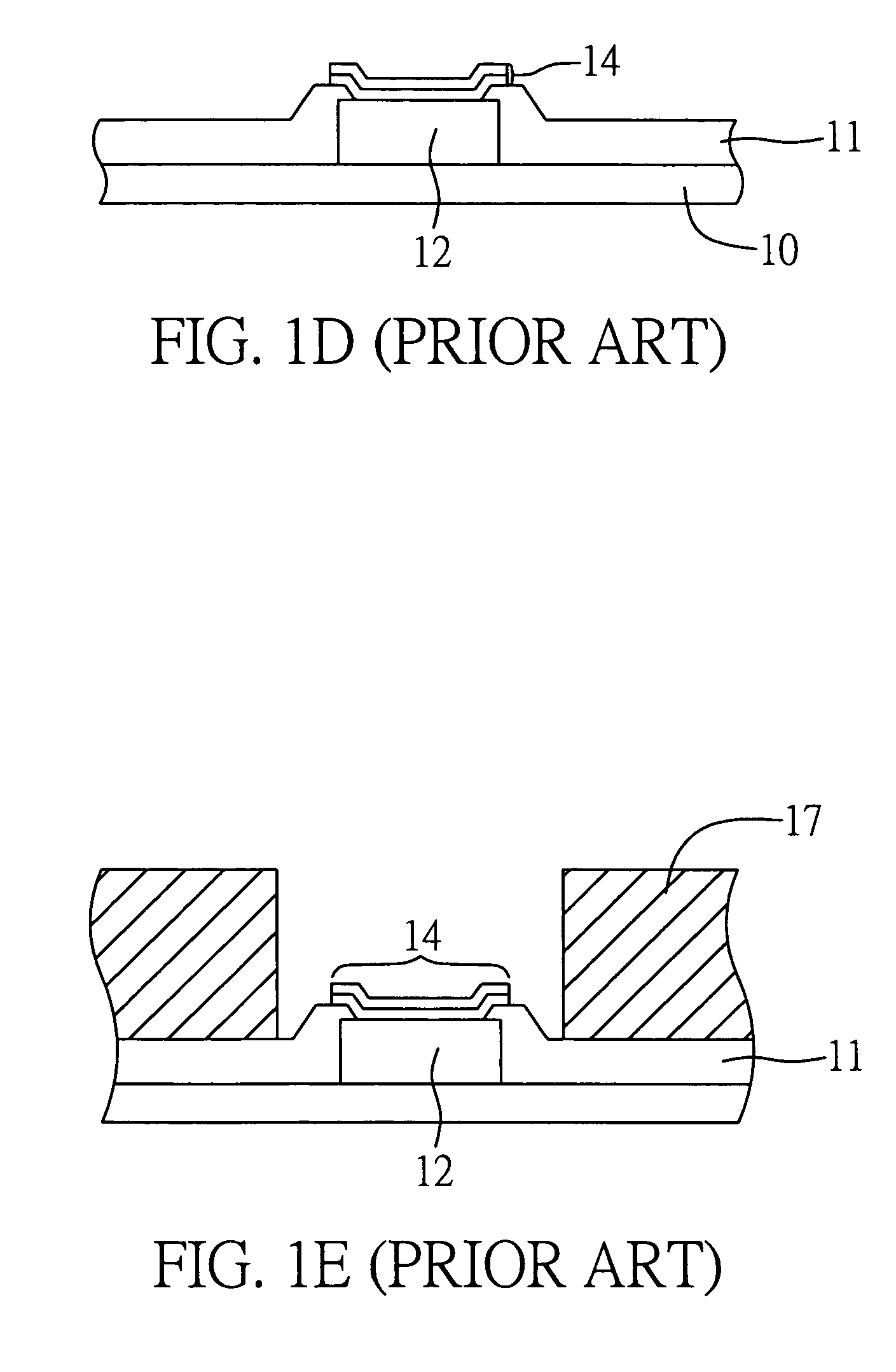
[0020]FIGS. 2A-2G show the procedural steps of a process for forming a copper-contained lead-free bump on an electronic component (such as chip) according to a first preferred embodiment of the present invention.

[0021]First, referring to FIG. 2A, a chip 20 is prepared having an active surface 20a on which a conductive trace layer including at least one bond pad 22 is formed. A passivation layer 21 is deposited on the conductive trace layer, with the bond pad 22 being exposed from the passivation layer 21. The passivation layer 21 is used to protect the conductive traces against external moisture and contaminants and electrically isolate the conductive traces from the outside.

[0022]Referring to FIG. 2B, an under bump metallurgy (UBM) structure 24 is formed over the passivation layer 21 and covers the bond pad 22. The UBM structure 24 comprises one or more metal layers that are usually made of aluminum-nickel / vanadium-copper (Al—Ni / V—Cu) alloy or a combination thereof, or can be selec...

second preferred embodiment

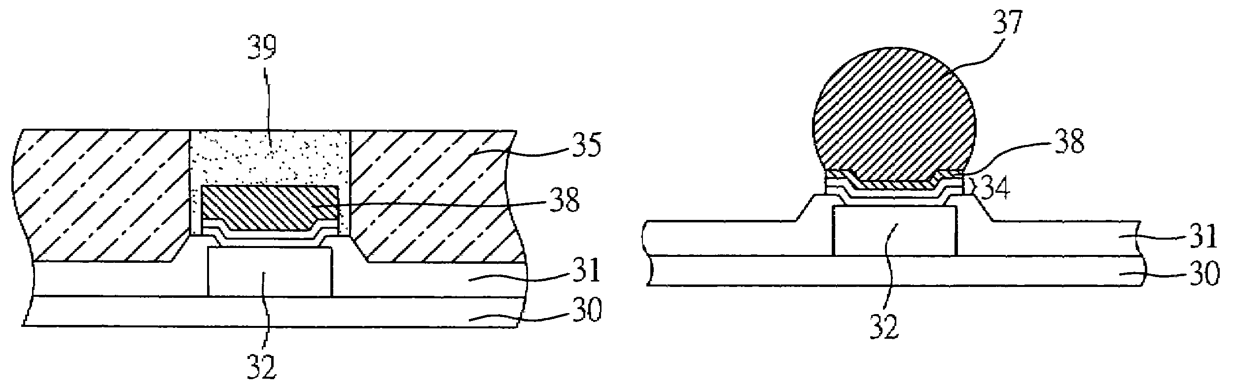
[0031]FIGS. 3A-3H show the procedural steps of the process for forming a copper-contained lead-free bump on an electronic component according to a second preferred embodiment of the present invention. The second embodiment differs from the above first embodiment in the aspects detailed below.

[0032]Referring to FIGS. 3A-3D, at least one bond pad 32 is formed on a chip 30, and a passivation layer 31 is applied over a surface 30a of the chip 30, with the bond pad 32 being exposed from the passivation layer 31. A UBM structure 34 is formed on the bond pad 32 and the passivation layer 31. A first photoresist 36 such as dry film is applied over the UBM structure 34 and has at least one opening corresponding in position to the bond pad 32. After a thick copper layer 38 is deposited by electroplating in the opening of the first photoresist 36, the first photoresist 36 and a part of the UBM structure 34 not covering the bond pad 32 are removed as shown in FIG. 3E, to expose the passivation l...


PUM

PropertyMeasurementUnit
thickaaaaaaaaaa
temperatureaaaaaaaaaa

Abstract

A process for forming a lead-free bump on an electronic component includes preparing the electronic component with at least one bond pad and a passivation layer formed thereon; forming an under bump metallurgy (UBM) structure on the passivation layer and the bond pad; applying a photoresist over the passivation layer, the photoresist having at least one opening corresponding to the bond pad; depositing a thick copper layer (about 1 to 10 μm thick) in the opening by electroplating; applying a copper-free or low-copper-content solder material on the copper layer; and performing a reflowing procedure under a suitable reflow temperature profile to allow copper ions to diffuse from the copper layer to the solder material so as to form the lead-free bump. This increases the copper content in the solder material but not raising the reflow temperature profile, thereby preventing deterioration of the photoresist due to over heat.

Description

FIELD OF THE INVENTION[0001]The present invention relates to processes for forming copper-contained lead-free bumps on electronic components, and more particularly, to a process for forming a copper-contained lead-free bump, which can use a low reflow temperature profile.BACKGROUND OF THE INVENTION[0002]Flip-chip ball grid array (FCBGA) semiconductor package is incorporated with both the flip-chip and BGA structures, in which an active surface of at least one chip is electrically connected to a surface of a substrate via a plurality of conductive bumps, and a plurality of solder balls are formed on an opposite surface of the substrate to serve as input / output (I / O) connections. The FCBGA package does not require conventional bonding wires, and can be effectively reduced in size, as well as may reduce the resistance to improve the electrical performance thereof, thereby making the FCBGA package become a mainstream packaging technology for chips and electronic elements of the next gen...

Claims


Application Information

Patent Timeline
Patent Type & Authority Patents(United States)
IPC IPC(8): H01L21/302H01L21/461H01L21/60H01L23/48H01L23/52H01L29/40
CPCH01L24/11H01L24/02H01L2224/0401H01L2224/03912H01L2224/1147H01L2224/11472H01L2224/11901H01L2224/11902H01L2224/13099H01L2924/01013H01L2924/01022H01L2924/01029H01L2924/01047H01L2924/01074H01L2924/01079H01L2924/01082H01L2924/01322H01L2924/01006H01L2924/01023H01L2924/01024H01L2924/01033H01L2924/014H01L24/03H01L24/05H01L2224/11462H01L2224/11502H01L2224/11849H01L2924/351H01L2924/00
Inventor CHIEN, FENG-LUNGCHANG, HUANG-CHUANHO, CHUN-SHENG
Owner SILICONWARE PRECISION IND CO LTD
Why Eureka
Try Eureka