METHOD FOR DEPOSITION OF MAGNESIUM DOPED (Al, In, Ga, B)N LAYERS

US20080042121A1Active Publication Date: 2008-02-21RGT UNIV OF CALIFORNIA

Image

  • METHOD FOR DEPOSITION OF MAGNESIUM DOPED (Al, In, Ga, B)N LAYERS
  • METHOD FOR DEPOSITION OF MAGNESIUM DOPED (Al, In, Ga, B)N LAYERS
  • METHOD FOR DEPOSITION OF MAGNESIUM DOPED (Al, In, Ga, B)N LAYERS

Examples


Embodiment Construction

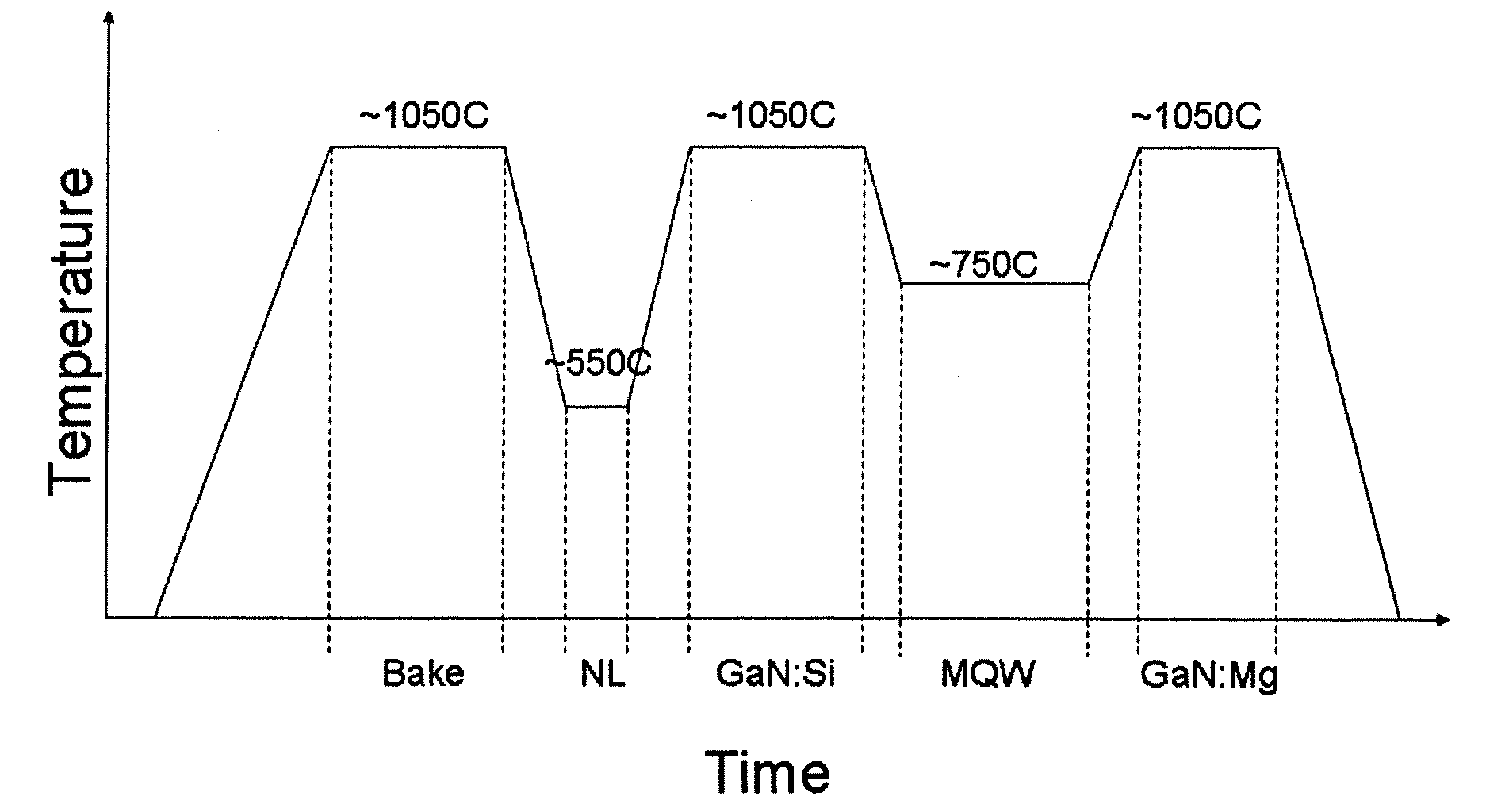
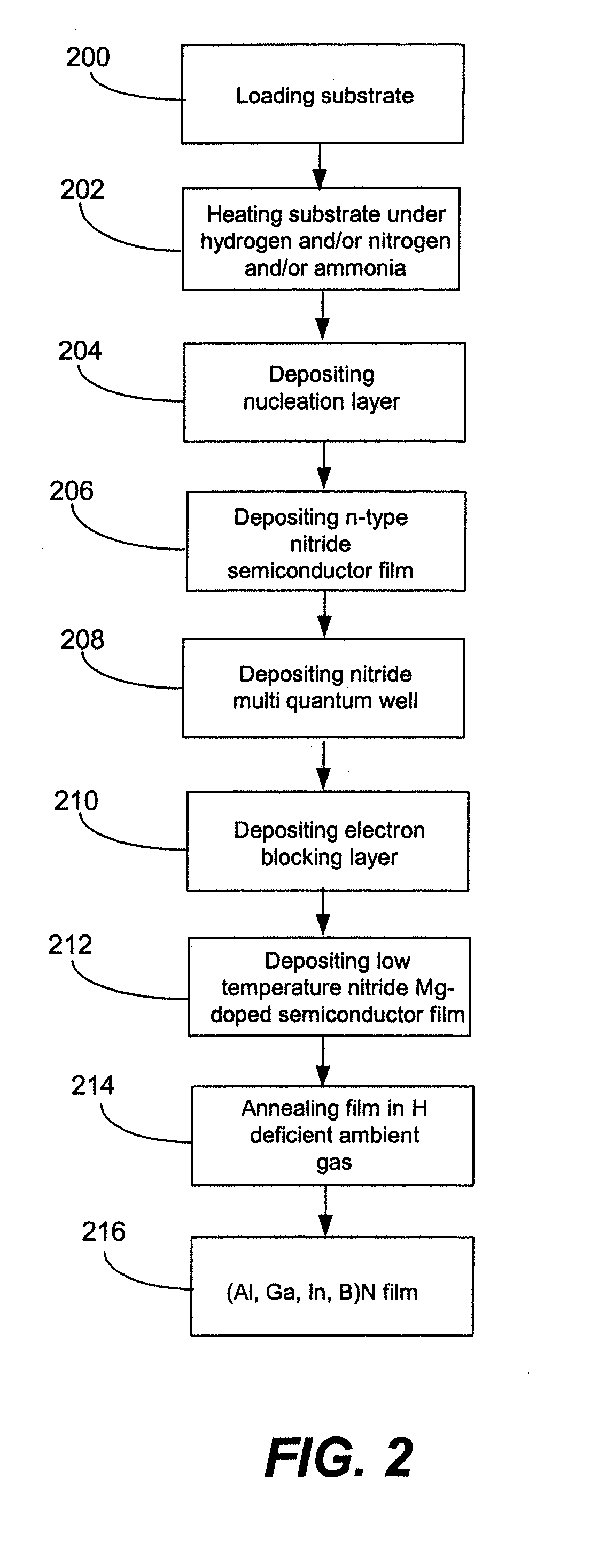
[0032]In the following description of the preferred embodiment, reference is made to the accompanying drawings which form a part hereof, and in which is shown by way of illustration a specific embodiment in which the invention may be practiced. It is to be understood that other embodiments may be utilized and structural changes may be made without departing from the scope of the present invention.

[0033]Overview

[0034]The present invention describes a method for growing device-quality, planar LT Mg doped nitride semiconductor thin films via MOCVD. Growth of LT Mg doped nitride semiconductor layers offers a means of improving device characteristics in III-nitride structures. The term nitrides refers to any alloy composition of the (Ga,Al,In,B)N semiconductors having the formula GanAlxInyBzN where:

0≦n≦1, 0≦x≦1, 0≦y≦1, 0≦z≦1, and n+x+y+z=1.

[0035]Current nitride devices, such as LEDs and LDs, comprise a high temperature grown (Al,In,Ga,B)N Mg doped layer. The high temperature Mg doped lay...


PUM


Abstract

A method for growing an improved quality device by depositing a low temperature (LT) magnesium (Mg) doped nitride semiconductor thin film. The low temperature Mg doped nitride semiconductor thin film may have a thickness greater than 50 nm. A multi quantum well (MQW) active layer may be grown at a growth temperature and the LT Mg doped nitride semiconductor thin film may deposited on the MQW active layer at a substrate temperature no greater than 150° C. above the growth temperature.

Description

CROSS-REFERENCE TO RELATED APPLICATION[0001]This application claims the benefit under 35 U.S.C. Section 119(e) of the following co-pending and commonly-assigned U.S. patent application:[0002]U.S. Provisional Application Ser. No. 60 / 822,600, filed on Aug. 16, 2006, by Michael Iza, Hitoshi Sato, Steven P. Denbaars and Shuji Nakamura, entitled “METHOD FOR DEPOSITION OF MAGNESIUM DOPED (Al, In, Ga, B)N LAYERS,” attorneys' docket number 30794.187-US-P1 (2006-678-1);[0003]which application is incorporated by reference herein.BACKGROUND OF THE INVENTION[0004]1. Field of the Invention[0005]This invention relates to a method for growing improved quality devices using low temperature magnesium doped nitride films.[0006]2. Description of the Related Art[0007](Note: This application references a number of different publications and patents as indicated throughout the specification by one or more reference numbers within brackets, e.g., [x]. A list of these different publications and patents ord...

Claims


Application Information

Patent Timeline
21 Feb 2008
Publication
US20080042121A1
IPC
H01L29/06; H01L21/20
CPC
B82Y20/00; H01L21/0242; H01L21/02458; H01L21/0254; H01L33/06; H01L21/02579; H01L21/02609; H01L21/0262
Inventors
IZA, MICHAEL; SATO, HITOSHI