Semiconductor device and BUS connecting method

Inactive Publication Date: 2008-02-21
FUJITSU MICROELECTRONICS LTD
View PDF7 Cites 0 Cited by
  • Summary
  • Abstract
  • Description
  • Claims
  • Application Information

AI Technical Summary

Benefits of technology

[0025]According to the semiconductor device as above, the write buffer and the read buffer in the bus interface circuit are accessible from the external bus, and the external bus's write access (read access) to the write buffer (read buffer) is used only during the external bus's write access (read access) to the first register, so that the external bus's write access (read access) to the second register can be completed within one cycle. Further, when the first internal resource is consti

Problems solved by technology

However, in the semiconductor device DEV of FIG. 1, two cycles are always needed for the external bus BUSE t

Method used


Image

  • Semiconductor device and BUS connecting method
  • Semiconductor device and BUS connecting method
  • Semiconductor device and BUS connecting method

Examples


Example

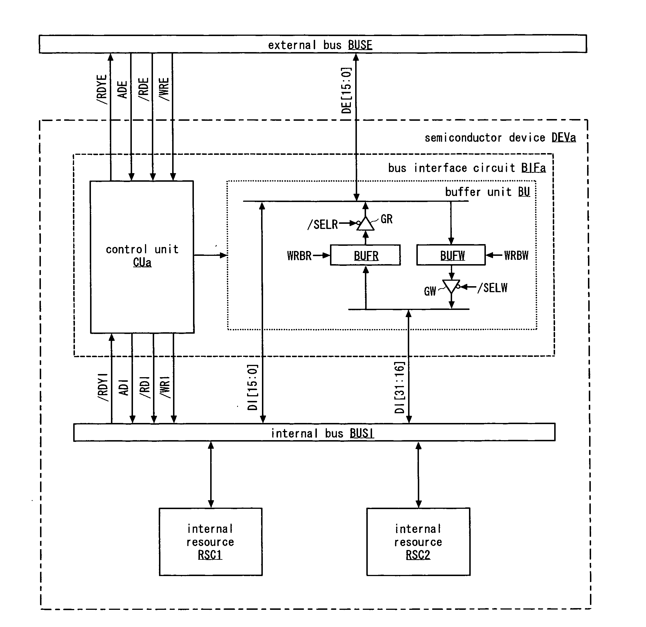
[0049]In the first embodiment as above, the write buffer BUFW and the read buffer BUFR in the bus interface circuit BIFa are accessible from the external bus BUSE, and the write access (read access) from the external bus BUSE to the write buffer BUFW (read buffer BUFR) is used only during the write access (read access) from the external bus BUSE to a register in the internal resource RSC1, so that the write access (read access) from the external bus BUSE to a register in the internal resource RSC2 can be completed by one cycle. Further, when writing same data to a plurality of registers in the internal resource RSC1, the data may be written to the write buffer BUFW by only a first cycle, so that a write access with the same data from the external bus BUSE to the plurality of registers in the internal resource RSC1 can be completed in a less number of cycles. Thus, the external access can be completed by a minimum number of cycles, which can contribute largely to improvement in effic...

Example

[0050]FIG. 12 shows a second embodiment of the present invention. FIG. 12 is explained below, but for the same elements as those explained with FIG. 1 and FIG. 7, the same symbols as those used in FIG. 1 and FIG. 7 are used, and detailed descriptions thereof are omitted. A semiconductor device DEVb of FIG. 12 is constituted by replacing the bus interface circuit BIFa in the semiconductor device DEVa of FIG. 7 with a bus interface circuit BIFb. The bus interface circuit BIFb is constituted of a control unit CUa and a buffer unit BUa. The buffer unit BUa is constituted by replacing the write buffer BUFW and the read buffer BUFR in the buffer unit BU with a read-write buffer BUFRW. The read-write buffer BUFRW functions as both the write buffer BUFW and the read buffer BUFR. Since no contention occurs between the write access and the read access by the external bus BUSE, the normality of the external access will not be lost even when the read-write buffer BUFRW is provided to replace th...


PUM


Abstract

A first internal resource has a first register which is accessible from an external bus via an internal bus and has a same data width as that of the internal bus which is larger than that of the external bus. A second internal resource has a second register which has a same data width as that of the external bus and is accessible from the external bus via the internal bus. A bus interface circuit implements a data transmitting operation between the external bus and the internal bus. The bus interface circuit is constituted of a write buffer and a read buffer which have a same data width as that of the external bus and are accessible from the external bus.

Description

CROSS REFERENCE TO RELATED APPLICATION[0001]This application is based upon and claims the benefit of priority from Japanese Patent Application No. 2006-223652, filed on Aug. 18, 2006, the entire contents of which are incorporated herein by reference.BACKGROUND OF THE INVENTION[0002]1. Field of the Invention[0003]The present invention relates to a semiconductor device having mounted together therein an internal resource which has a register having a data width (number of bits) larger than a data width of an external bus and an internal resource which has a register having a same data width as the external bus, and it relates to a bus connecting method of connecting the external bus and the internal bus in the semiconductor device.[0004]2. Description of the Related Art[0005]There is a semiconductor device whose external bus and internal bus have different data widths. For example, in a case where the data width of an external bus is 16 bits and the data width of the internal bus is 3...

Claims


Application Information

Patent Timeline
IPC IPC(8): G06F13/40
CPCG06F13/4018
Inventor ISHIZUKA, MASANORIHOSOI, TOSHIO
Owner FUJITSU MICROELECTRONICS LTD
Why Eureka
Try Eureka