Single-Poly Non-Volatile Memory Cell

a non-volatile memory, single-poly technology, applied in the field of non-volatile memory, can solve the problems of increasing manufacturing costs, prone to junction breakdown of buried diffusion regions, and reducing device density

Active Publication Date: 2008-04-10
SIEMENS PROD LIFECYCLE MANAGEMENT SOFTWARE INC
View PDF16 Cites 9 Cited by
  • Summary
  • Abstract
  • Description
  • Claims
  • Application Information

AI Technical Summary

Benefits of technology

[0009]The scope of the invention is defined by the claims, which are incorporated into this section by reference. A more complete understanding of embodiments of the present invention will be afforded to those skilled in the art, as well as a realization of additional advantages thereof, by a consideration of the following detailed description of one or more embodiments. Reference will be made to the appended sheets of drawings that will first be described briefly.

Problems solved by technology

Although conventional single-poly non-volatile memory cells are compatible with CMOS manufacturing processes, the buried diffusion area occupies die area and thus decreases device density, thereby increasing manufacturing costs.
Moreover, the buried diffusion region is prone to junction breakdown.
However, forming a trench MIM capacitor demands extra processing steps and thus also increases costs.

Method used


Image

  • Single-Poly Non-Volatile Memory Cell
  • Single-Poly Non-Volatile Memory Cell
  • Single-Poly Non-Volatile Memory Cell

Examples


Embodiment Construction

[0015]Reference will now be made in detail to one or more embodiments of the invention. While the invention will be described with respect to these embodiments, it should be understood that the invention is not limited to any particular embodiment. On the contrary, the invention includes alternatives, modifications, and equivalents as may come within the spirit and scope of the appended claims. Furthermore, in the following description, numerous specific details are set forth to provide a thorough understanding of the invention. The invention may be practiced without some or all of these specific details. In other instances, well-known structures and principles of operation have not been described in detail to avoid obscuring the invention.

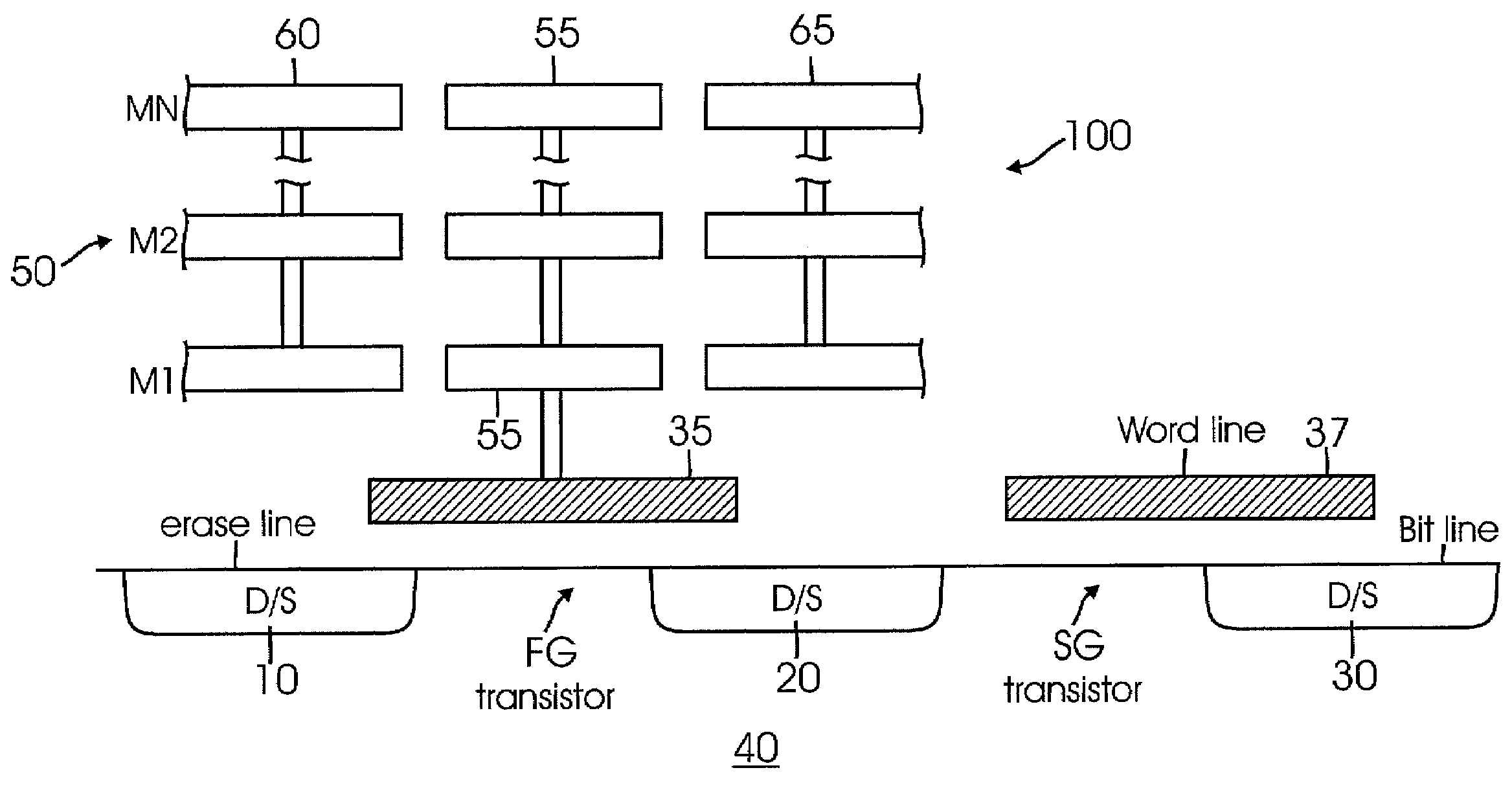
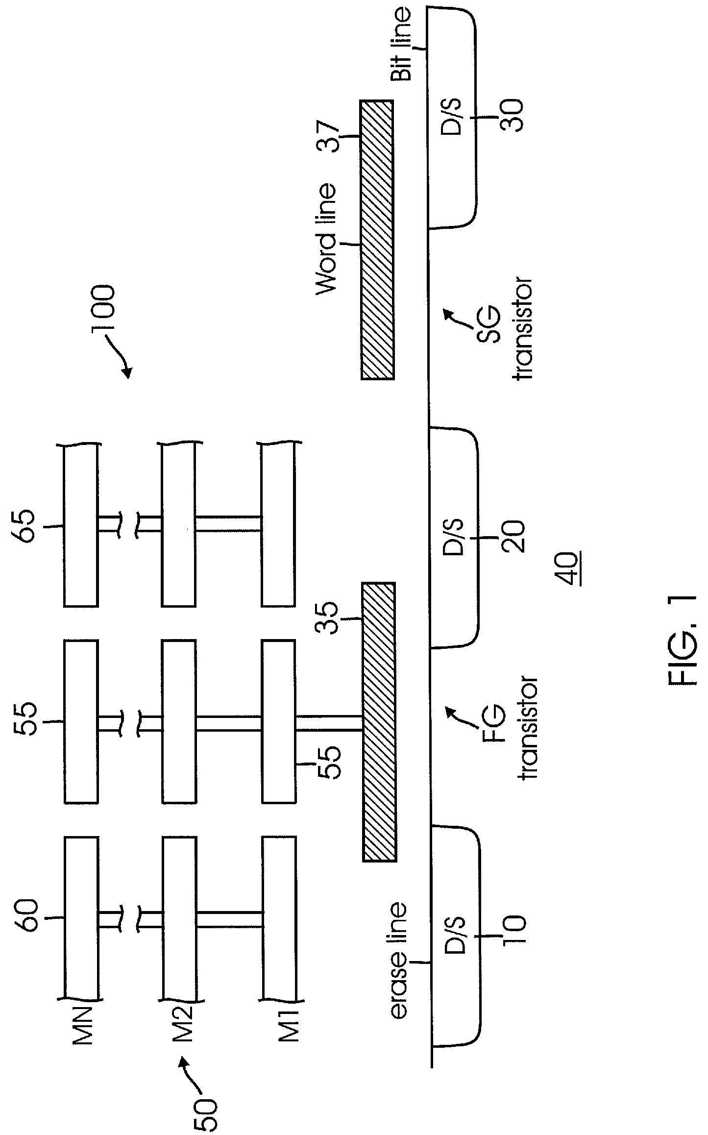
[0016]Turning now to the drawings, FIG. 1 illustrates a non-volatile memory cell 100 in which the control gate is formed using semiconductor metal routing layers M1 through MN. These metal routing layers are already present in conventional CMOS se...


PUM


Abstract

A non-volatile memory cell includes a floating gate transistor having a floating gate coupled to a metal layer capacitor defined in one or more metal layers. Within each metal layer, the metal layer capacitor includes a first plate coupled to the floating gate and a second plate separated from the first plate by a fringe capacitance junction.

Description

TECHNICAL FIELD[0001]This application relates generally to non-volatile memory, and more particularly to a non-volatile memory in which a floating gate is programmed and erased using fringe capacitance.BACKGROUND OF THE INVENTION[0002]Non-volatile memory cells include a floating gate in which electric charge may be injected. As implied by the name, the floating gate electrically “floats” with regard to other structures in the cell such that the injected charge is retained even if the memory cell is powered down. In a classic non-volatile memory cells, two separate polysilicon layers are required. A first polysilicon layer forms the floating gate. A second overlaying polysilicon layer forms a control gate that is used to program the floating gate. Because CMOS semiconductor manufacturing processes provide only a single polysilicon layer, “single-poly” non-volatile memory cells have been developed in which the control gate is formed as a buried diffusion region.[0003]Although conventi...

Claims


Application Information

Patent Timeline
Patent Type & Authority Applications(United States)
IPC IPC(8): H01L29/788G11C11/24
CPCG11C16/0433H01L27/11521H01L27/115G11C2216/10H10B69/00H10B41/30
Inventor TERZIOGLU, ESINWINOGRAD, GIL I.AFGHAHI, MORTEZA CYRUS
Owner SIEMENS PROD LIFECYCLE MANAGEMENT SOFTWARE INC
Why Eureka
Try Eureka