Edge exposure apparatus, coating and developing apparatus, edge exposure method and coating and developing method, and storage medium

a technology of exposure apparatus and film, applied in the direction of photosensitive materials, instruments, printers, etc., can solve the problems of deteriorating cut width of film to be removed, difficult to sharply cut resist film at the edge portion of the wafer, and particle defects, etc., to achieve high cut width accuracy and shape the effect of width

Inactive Publication Date: 2008-04-17
TOKYO ELECTRON LTD
View PDF3 Cites 7 Cited by
  • Summary
  • Abstract
  • Description
  • Claims
  • Application Information

AI Technical Summary

Benefits of technology

[0013]The present invention is made under such circumstances. An object of the present invention is to provide a technique that allows an unnecessary coating film at an edge portion of a substrate to be removed with high accuracy of shape and width.

Problems solved by technology

If a resist film is present here, the resist film adheres to the transport arm and then peels off from the transport arm in a transport step, resulting in particles which are a cause of defects.
However, in the edge rinse using an organic solvent, because of the compatibility between organic solvents and coating films, with some kinds of resist film, it is difficult to sharply cut the resist film at the edge portion of the wafer in such a manner in that the end portion is linearly shaped.
In the edge rinse using an organic solvent, because of the compatibility between the resist liquid and the organic solvent as described above, the accuracy of cut width of a film to be removed is deteriorated or the shape of the cut surface is deteriorated.
However, since the unnecessary resist film at the edge portion cannot be removed without a development process after the exposure process, the resist film may attach to a transport arm and cause particles in the transport step before the development process, as described above.
In addition, in the liquid immersion exposure process, the resist film present at the edge portion of the wafer comes in contact with water, which may cause film peeling.

Method used


Image

  • Edge exposure apparatus, coating and developing apparatus, edge exposure method and coating and developing method, and storage medium
  • Edge exposure apparatus, coating and developing apparatus, edge exposure method and coating and developing method, and storage medium
  • Edge exposure apparatus, coating and developing apparatus, edge exposure method and coating and developing method, and storage medium

Examples


Embodiment Construction

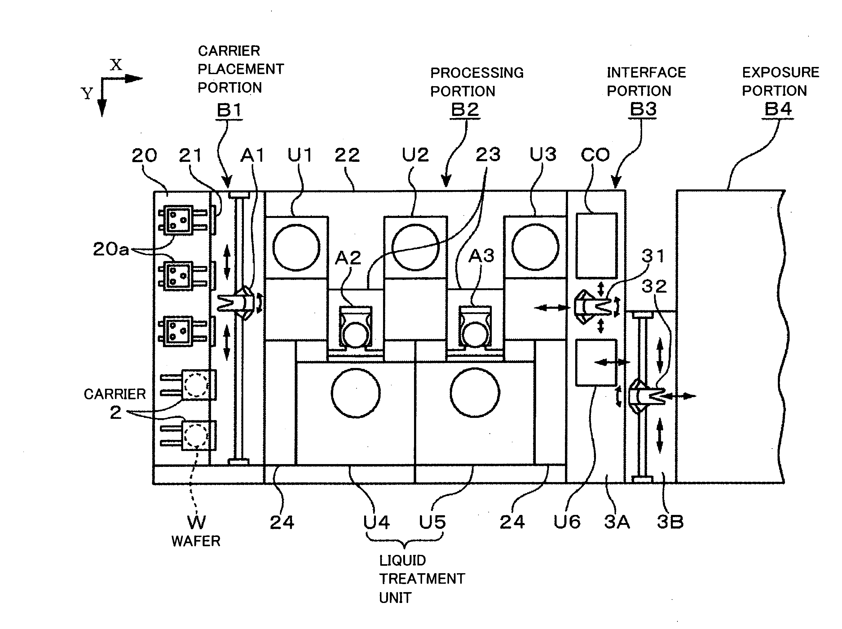
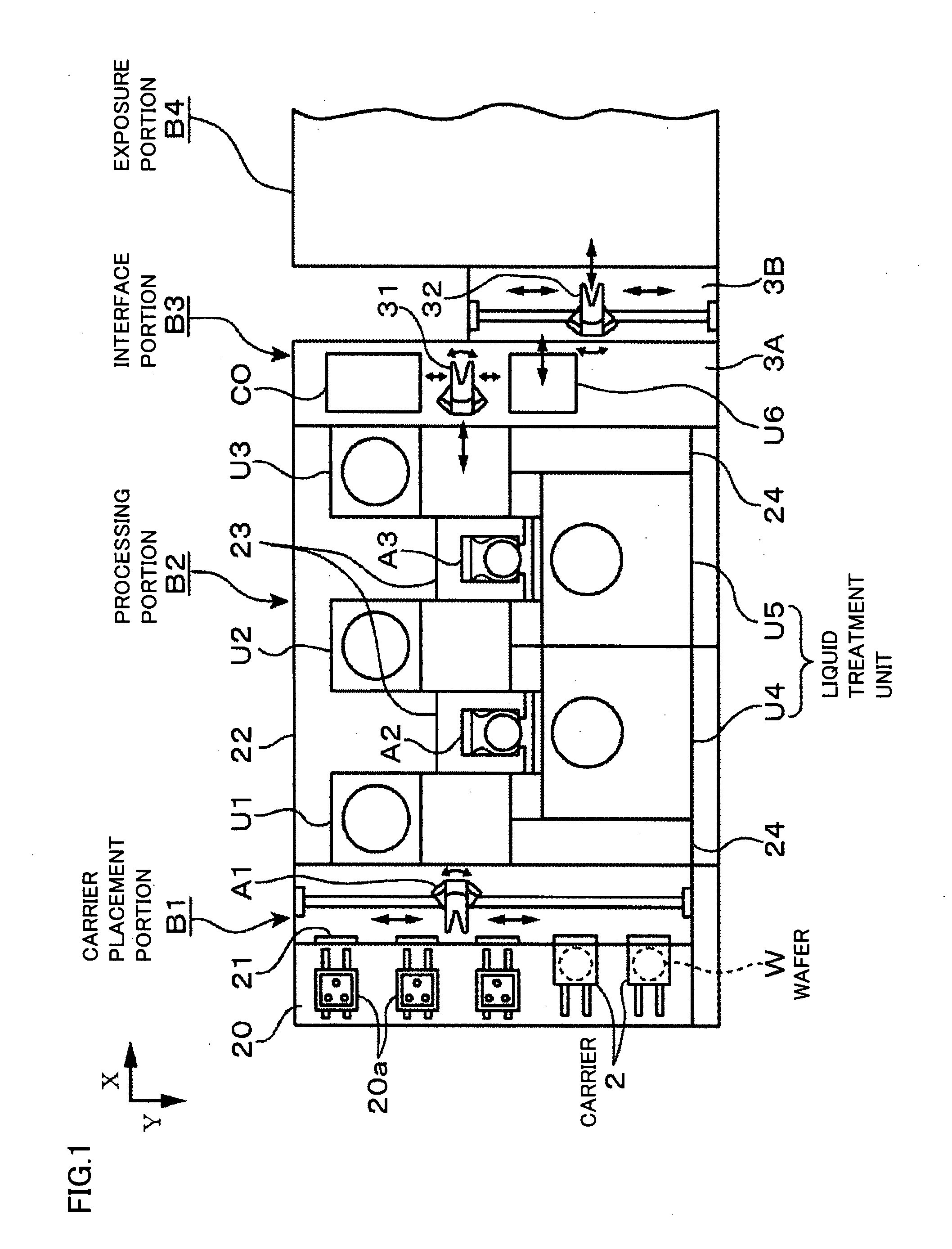
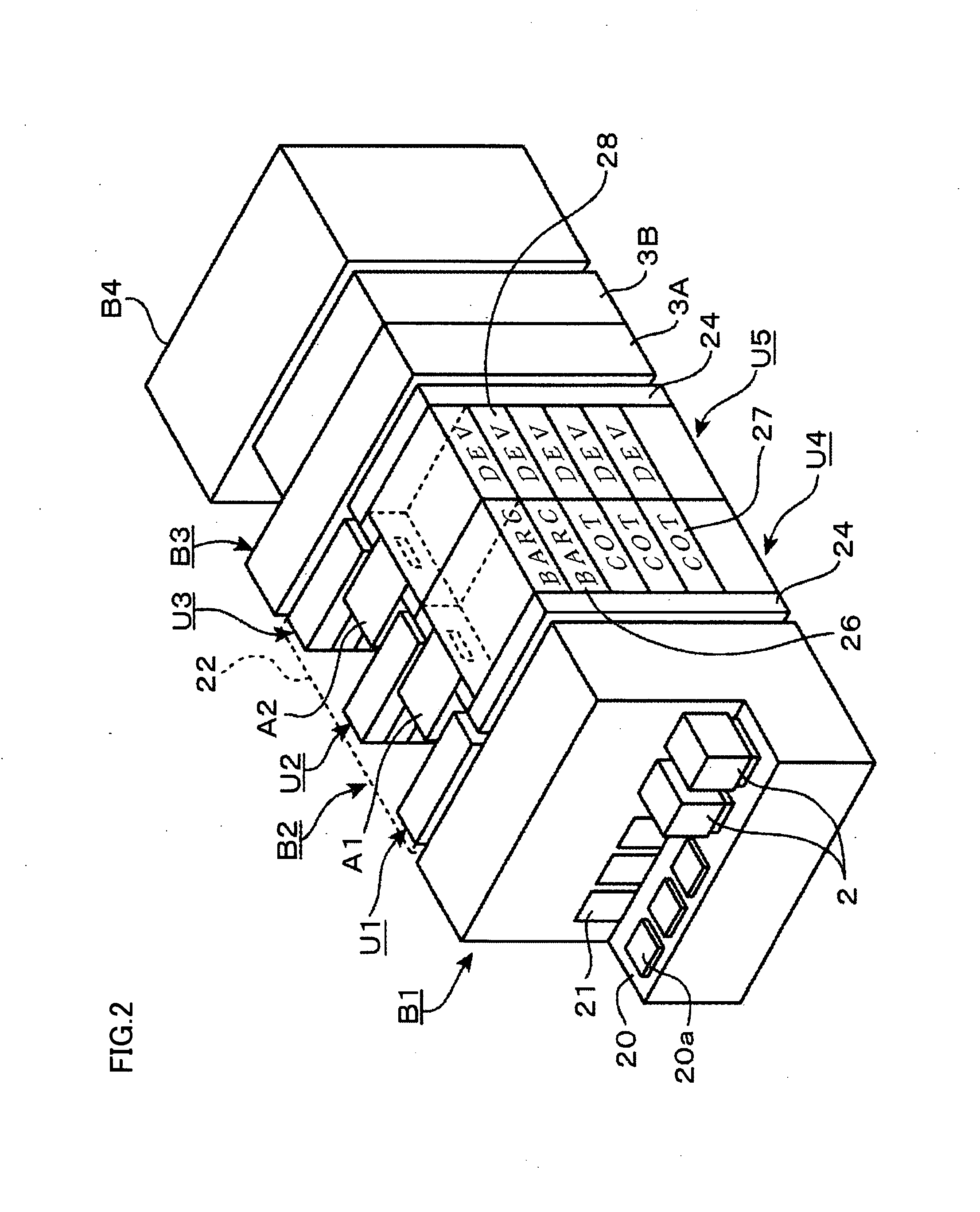
[0037]First, with reference to FIG. 1 and FIG. 2, an overall configuration of a resist pattern formation system in which an exposure apparatus is connected to a coating and developing apparatus having an edge exposure apparatus of the present invention built therein will be described briefly. The figures show a carrier placement portion B1 for carrying in / out a carrier 2 hermetically accommodating substrates, for example, 13 wafers W. In carrier placement portion B1, provided are a carrier station 20 including a placement portion 20a on which a plurality of carriers 2 can be placed side by side, an opening / closing portion 21 provided on a front wall surface as viewed from carrier station 20, and delivery means A1 for taking out wafer W from carrier 2 through opening / closing portion 21.

[0038]At the back of carrier placement portion B1, a processing portion B2 enclosed with a casing 22 is connected. In this processing portion B2, shelf units U1, U2, U3 comprised of multiple stages of ...


PUM

PropertyMeasurementUnit
wavelengthaaaaaaaaaa
ejection pressureaaaaaaaaaa

Abstract

An edge exposure apparatus performing an exposure process on an edge portion of a wafer having a coating film (resist film) formed thereon includes position detection means for detecting positional data of an outer edge of a wafer held by a spin chuck, an exposure portion for performing an exposure process on the edge portion of the wafer, a development nozzle supplying a developer to the exposed region, and alignment means for horizontally moving the spin chuck. An exposure process is performed by the exposure portion on the edge portion of the wafer held by the spin chuck while the alignment means is controlled, based on the positional data of the outer edge of the wafer which is detected by the position detection means, such that the positional relation between the outer edge of the wafer and the exposure portion is kept constant.

Description

BACKGROUND OF THE INVENTION[0001]1. Field of the Invention[0002]The present invention relates to a technique for removing an unnecessary coating film at an edge portion, for example, of a substrate having a coating film formed thereon.[0003]2. Description of the Background Art[0004]In a manufacturing process of semiconductor devices and LCD substrates, a resist pattern is formed on a substrate by a technique called photolithography. This technique is performed, for example, through a series of steps of applying a resist liquid on a substrate such as a semiconductor wafer (referred to as a wafer hereinafter), exposing the resist in a prescribed pattern, and thereafter performing a development process to obtain a desired pattern. Such a process is generally performed using a system in which an exposure apparatus is connected to a coating and developing apparatus for applying and developing a resist liquid.[0005]Recently, as device patterns are increasingly reduced in size and film thi...

Claims


Application Information

Patent Timeline
Patent Type & Authority Applications(United States)
IPC IPC(8): G03B27/52G03C5/00
CPCG03F7/2028G03B27/52
Inventor KOSUGI, HITOSHIYAMAMOTO, TAROYAMADA, YOSHIAKISAIGA, YASUHITO
Owner TOKYO ELECTRON LTD
Why Eureka
Try Eureka