Sub-lithographic NANO interconnect structures, and method for forming same

a sub-lithographic nano and interconnect structure technology, applied in the direction of material nanotechnology, semiconductor devices, semiconductor/solid-state device details, etc., can solve the problems of low device density of integrated circuits, limited line and/or via opening dimensions, and inability to meet the requirements of lithographic tools

Inactive Publication Date: 2008-04-24
ELPIS TECH INC
View PDF1 Cites 166 Cited by
  • Summary
  • Abstract
  • Description
  • Claims
  • Application Information

AI Technical Summary

Benefits of technology

[0028]The term “self-aligned” is used in the present application to denote that the via and line openings are formed using one lithographically defined hard mask and the alignment error between the via and line openings is smaller than that between two lithographic masks.
[0029]Other aspects, features and advantages of the invention will be more fully apparent from the ensuing disclosure and appended claims.

Problems solved by technology

As such, the dimensions of the line and / or via openings are limited to the resolution of the lithographic tool.
Such large opening diameters contribute to undesirable low device density of the integrated circuit.

Method used


Image

  • Sub-lithographic NANO interconnect structures, and method for forming same
  • Sub-lithographic NANO interconnect structures, and method for forming same
  • Sub-lithographic NANO interconnect structures, and method for forming same

Examples


Embodiment Construction

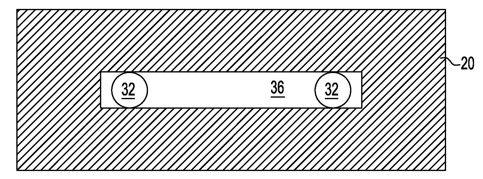
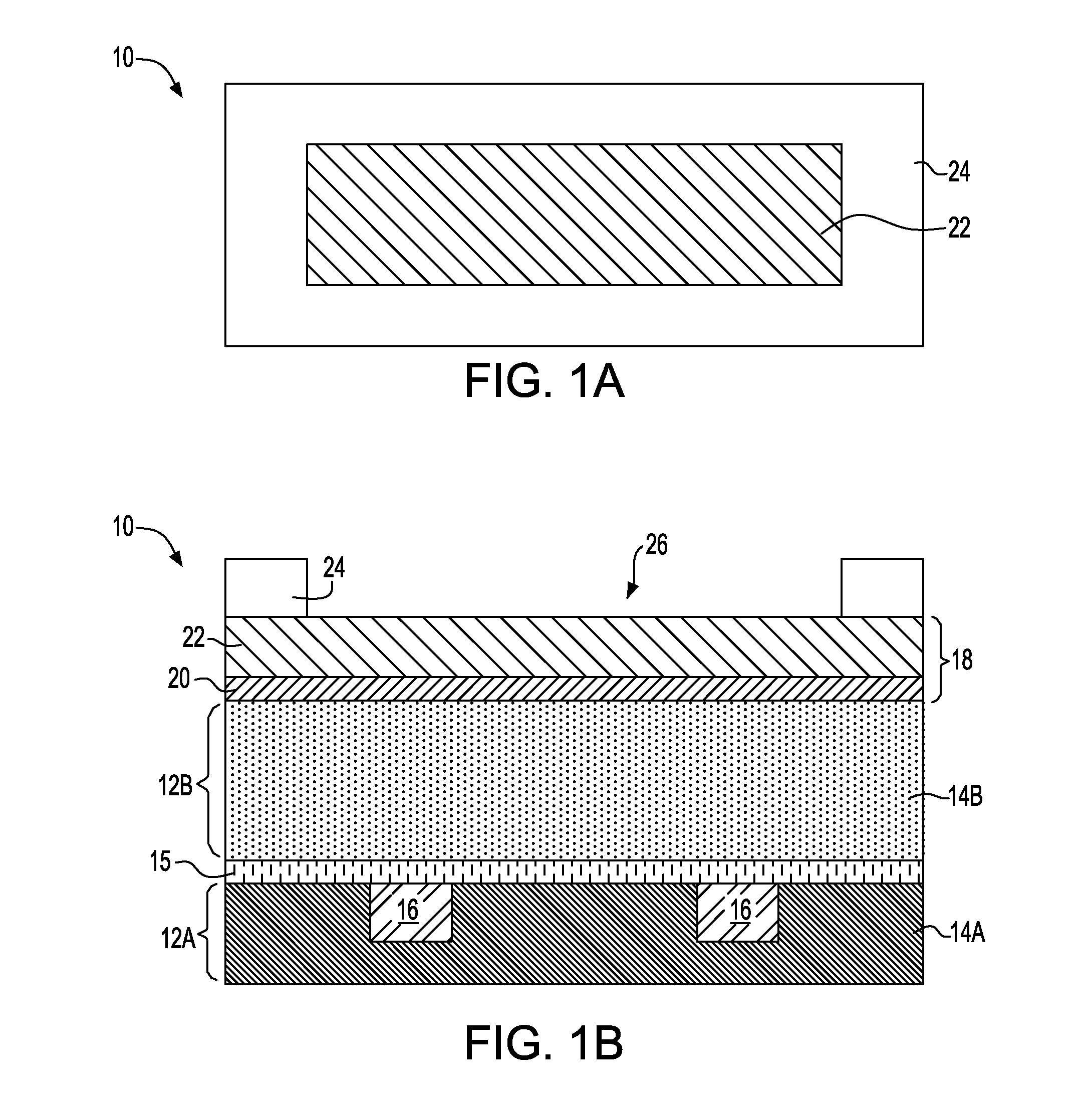
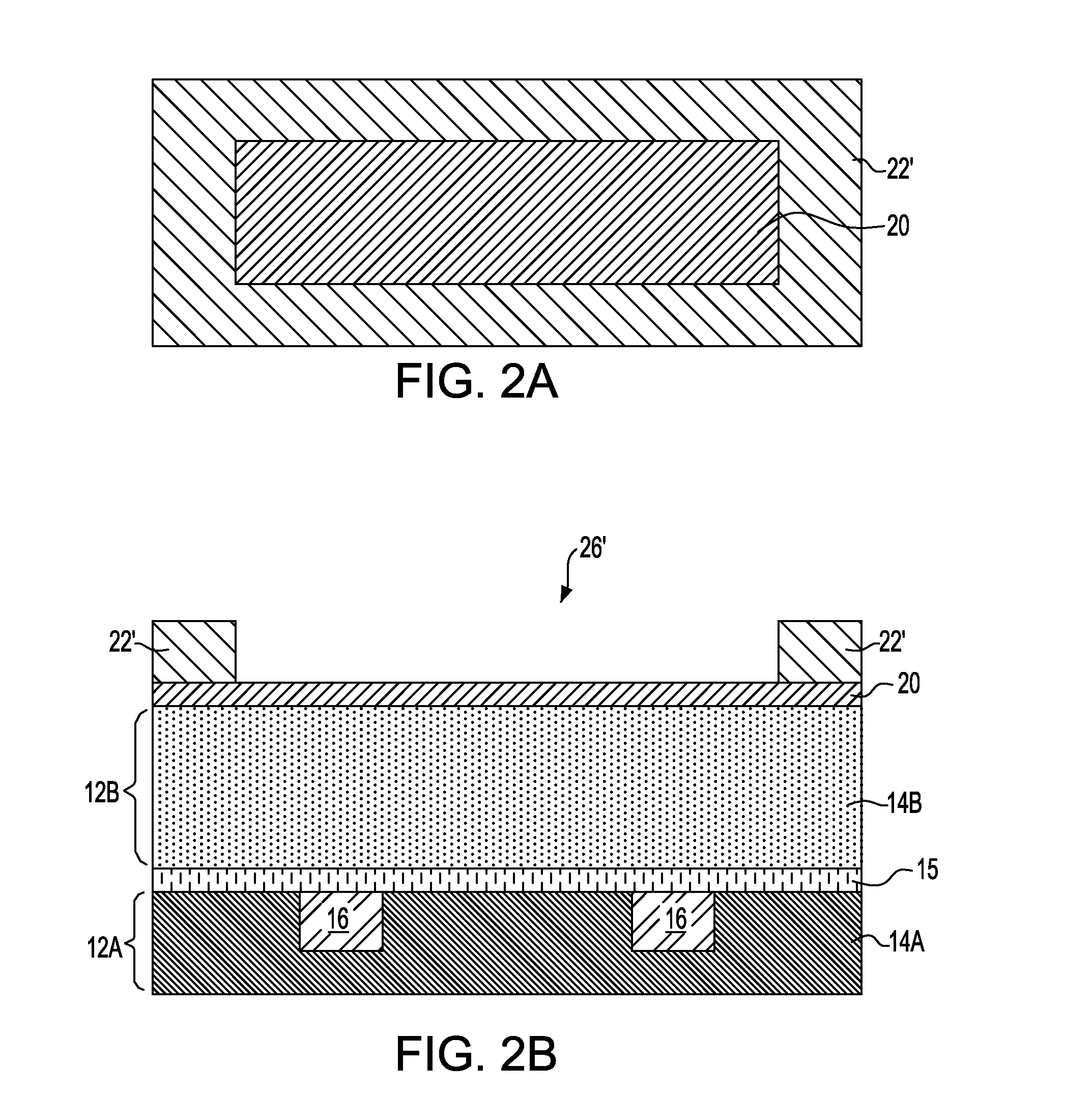
[0048]The present invention, which provides an interconnect structure including nano-scale, e.g., sub-lithographic, lines and vias and a method of fabricating the same, will now be described in greater detail by referring to the following description and drawings that accompany the present application. It is noted that the drawings of the present invention are provided for illustrative purposes and, as such, they are not drawn to scale.

[0049]In the following description, numerous specific details are set forth, such as particular structures, components, materials, dimensions, processing steps and techniques, in order to provide a thorough understanding of the present invention. However, it will be appreciated by one of ordinary skill in the art that the invention may be practiced without these specific details. In other instances, well-known structures or processing steps have not been described in detail in order to avoid obscuring the invention.

[0050]It will be understood that whe...


PUM


Abstract

A method to form interconnect structures including nano-scale, e.g., sub-lithographic, lines and vias for future generation of semiconductor technology using self-assembly block copolymers that can be placed at a specific location using a pre-fabricated hard mask pattern is provided. The inventive method provides an interconnect structure in which the line is self-aligned to the via.

Description

FIELD OF THE INVENTION[0001]The present invention relates to a semiconductor structure and a method of fabricating the same. More particularly, the present invention relates to an interconnect structure including nano-scale conductively filled openings and a method of fabricating the same.BACKGROUND OF THE INVENTION[0002]Generally, semiconductor devices include a plurality of circuits which form an integrated circuit fabricated on a semiconductor substrate. A complex network of signal paths will normally be routed to connect the circuit elements distributed on the surface of the substrate. Efficient routing of these signals across the device requires formation of multilayered schemes. These interconnect structures typically include copper, Cu, since Cu based interconnects provide higher speed signal transmission between large numbers of transistors on a complex semiconductor chip as compared to aluminum-based interconnects.[0003]Within a typical interconnect structure, metal vias ru...

Claims


Application Information

Patent Timeline
Patent Type & Authority Applications(United States)
IPC IPC(8): H01L23/52H01L21/4763
CPCB81C1/00095B81C2201/0149H01L2924/0002B81C2201/0198B82Y30/00H01L21/0337H01L21/0338H01L21/31144H01L21/76808H01L21/76811H01L21/76813H01L23/5329H01L23/53295H01L2924/00H01L21/76816
Inventor YANG, HAININGLI, WAI-KIN
Owner ELPIS TECH INC
Why Eureka
Try Eureka