Semiconductor Device

Inactive Publication Date: 2008-06-05
SEMICON ENERGY LAB CO LTD
View PDF41 Cites 8 Cited by
  • Summary
  • Abstract
  • Description
  • Claims
  • Application Information

AI Technical Summary

Benefits of technology

[0011]According to the present invention, a transistor is provided, in which a semiconductor layer is thin, and a channel length is ten times or more and less than forty times the thickness of the semiconductor layer or is 100 nm or more and l

Problems solved by technology

However, in the case where the gate electrode is formed to have a complicated shape in miniaturizing an integrated circuit, difficulty in the manufacturing process is increased.
In addi

Method used


Image

  • Semiconductor Device
  • Semiconductor Device
  • Semiconductor Device

Examples


Embodiment Construction

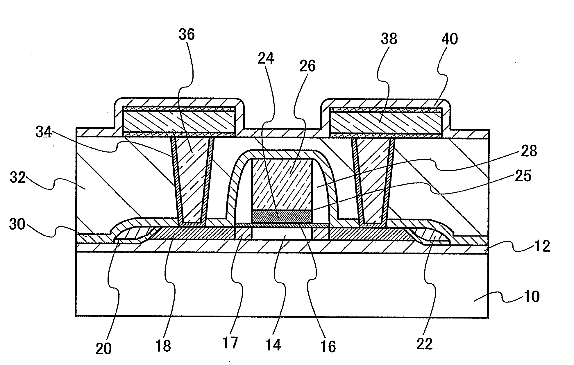
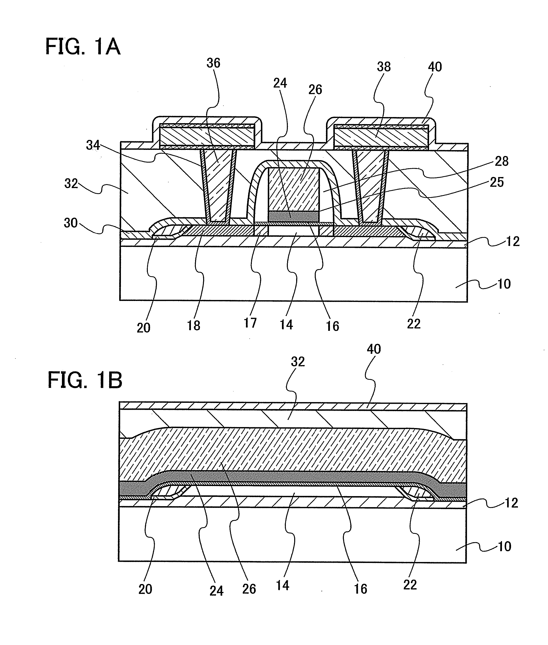
[0022]Embodiment mode of the present invention will be described with reference to the accompanying drawings. However, the present invention can be implemented in various ways, and it is easily understood by those skilled in the art that various changes and modifications are possible, unless such changes and modifications depart from the sprit and the scope of the invention. Therefore, the present invention is not construed as being limited to the description of the following embodiment mode. It is to be noted that like portions in the drawings of the present invention to be given below may be denoted by like reference numerals in the drawings.

[0023]FIGS. 1A and 1B show a structure of a field effect transistor that is a main component of a semiconductor device of the present invention. FIG. 1A is a cross-sectional view of the field effect transistor in a channel length direction, and FIG. 1B is a cross-sectional view thereof in a channel width direction (direction perpendicular to t...


PUM


Abstract

A semiconductor device has a so-called SOI structure in which an element is constituted by a semiconductor layer on an insulating surface, and the semiconductor layer is extremely thin as 5 nm to 30 nm. The semiconductor device is provided with a field effect transistor that includes in addition to such a semiconductor layer, a gate insulating layer with a thickness of 2 nm to 20 nm and a gate electrode, and a channel length is ten times or more and less than 40 times the thickness of the semiconductor layer. When the semiconductor layer is formed to be thin, the semiconductor device operates so as not to be easily influenced by a concentration of impurity imparting one conductivity type added to a channel formation region.

Description

BACKGROUND OF THE INVENTION[0001]1. Field of the Invention[0002]The present invention relates to a semiconductor device formed using a semiconductor layer provided on an insulating surface, and particularly a miniaturization technique for a field effect transistor.[0003]2. Description of the Related Art[0004]A method is known, in which miniaturization of a thin film transistor (hereinafter, also referred to as “TFT”) that is one kind of filed effect transistors is attempted by shortening a channel length represented as a distance between a source and a drain in order to achieve high performance. This is a method in which high-speed operation is attempted by shortening a traveling distance of carriers flowing through a channel of the transistor.[0005]However, when the channel length is shortened, a phenomenon that threshold voltage is changed and leak current is increased between the source and the drain in a weak inversion state, which is a so-called short-channel effect, becomes pr...

Claims


Application Information

Patent Timeline
IPC IPC(8): H01L29/04
CPCH01L27/12H01L29/78696H01L27/1214
Inventor YAMAZAKI, SHUNPEIARAI, YASUYUKI
Owner SEMICON ENERGY LAB CO LTD
Why Eureka
Try Eureka