Multi-Band Antenna, Circuit Board And Communication Device
a multi-band antenna and circuit board technology, applied in the direction of antenna supports/mountings, resonant antennas, radiating element structural forms, etc., can solve the problems of difficult downsizing, difficult to reduce, and complicated band switching mechanism of such antenna devices
- Summary
- Abstract
- Description
- Claims
- Application Information
AI Technical Summary
Benefits of technology
Problems solved by technology
Method used
Image
Examples
embodiment 1
[0091]Next, an embodiment of the multi-band antenna of the present invention will be explained specifically.
[0092]Here, a multi-band antenna downsized so as to be suitably incorporated into the communication device will be exemplified. FIG. 11 is a external perspective view (main part) of a base for mounting the multi-band antenna to the communication device and FIG. 12 is a side view of the base seen from a direction of arrow of FIG. 11. In those figures, components considered to be same or understood to be same with those already described will be denoted by the same reference numerals for convenience.
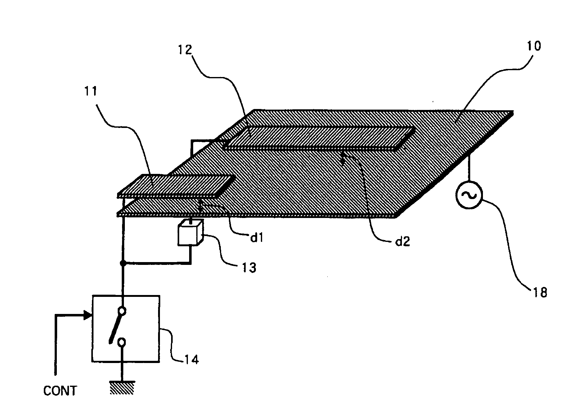
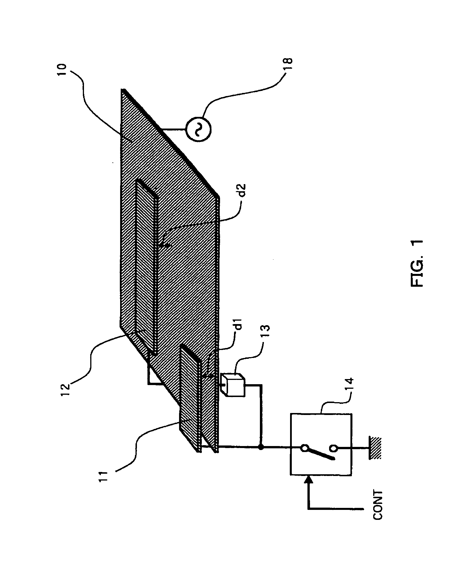
[0093]The multi-band antenna of this embodiment is constructed by mounting the main element 10 having a shape of inversed F, for example, on a dielectric board such as a base 60 made of epoxy glass (FR-4) provided on an edge portion of the ground conductor 50 to which the earth terminal of the switching mechanism 14 is connected. Then, an element mounting cover 70 made of epoxy glass...
embodiment 2
[0108]Next, another embodiment of the present invention will be explained. While the example described above is an example in which the multi-band antenna is implemented mainly as an antenna part incorporated in the communication device and the like, the multi-band antenna may be implemented as conductive plating and a conductive pattern directly formed on a circuit board composing the communication device and the like.
[0109]That is, as shown in FIG. 19(a), a front surface section of an antenna area of a circuit board 80 is plated by the conductive plate for example to set the plated part as the main element 10 and an approximately rectangular conductive pattern is formed near an end portion of a back surface section of the antenna area of the circuit board 80 and a lengthy thin plate conductive pattern is formed approximately near the center thereof, respectively, by etching as shown in FIG. 19(b) so that the former functions as the first sub-element 11 and the latter as the second...
PUM
 Abstract
Description
Claims
Application Information


