Memory chip and insert card having the same thereon

a memory chip and insert card technology, applied in the direction of instruments, electrical apparatus casings/cabinets/drawers, semiconductor/solid-state device details, etc., can solve the problems of difficult installation and removal of small-size memory chips from the motherboard

Inactive Publication Date: 2008-06-12
KRETON CORP
View PDF3 Cites 27 Cited by
  • Summary
  • Abstract
  • Description
  • Claims
  • Application Information

AI Technical Summary

Problems solved by technology

However, small size memory chips are difficult to be installed and removed from the motherboard, especially when the welding points are located between the memory chips and the motherboard.

Method used


Image

  • Memory chip and insert card having the same thereon
  • Memory chip and insert card having the same thereon
  • Memory chip and insert card having the same thereon

Examples


Embodiment Construction

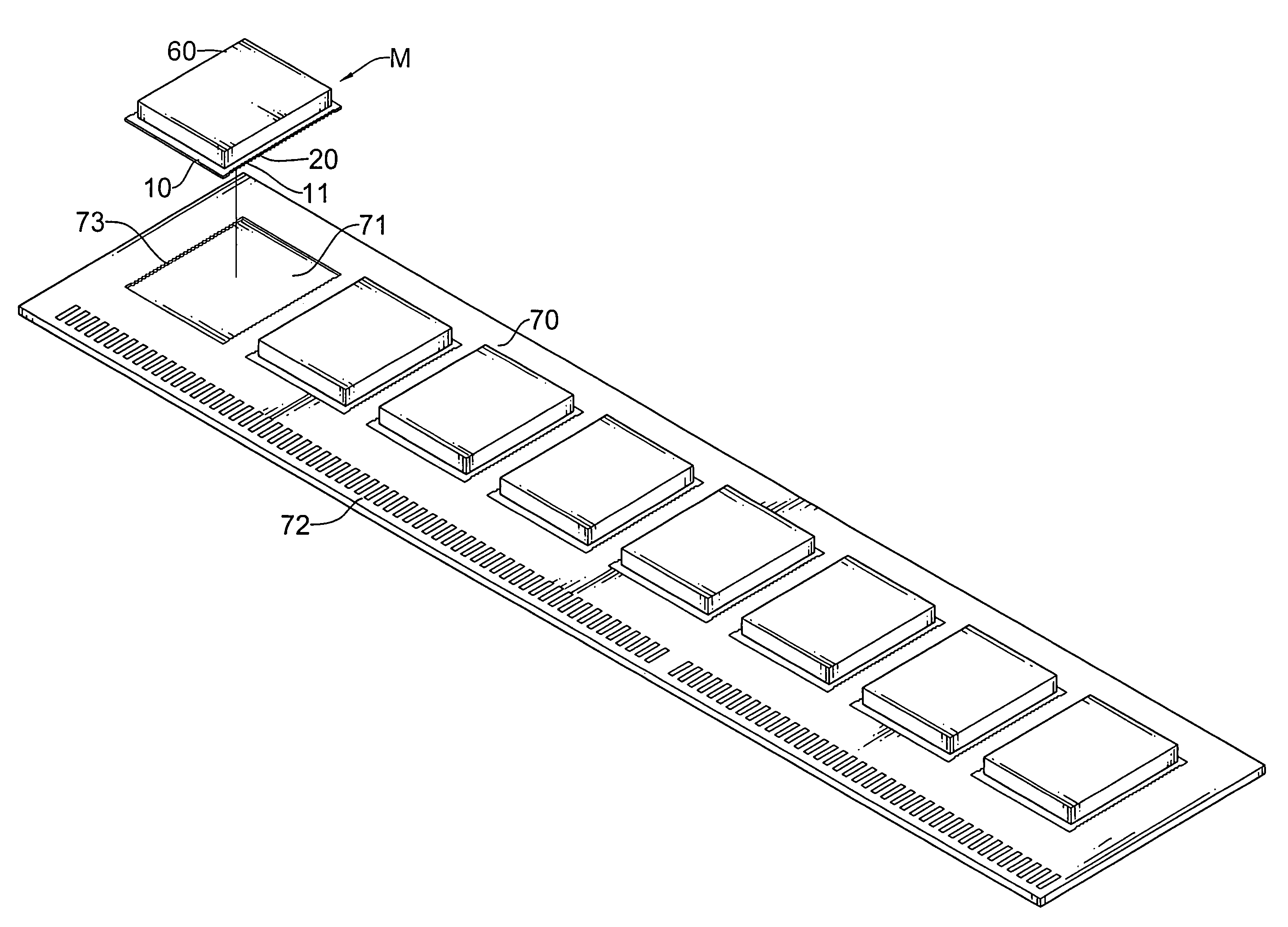
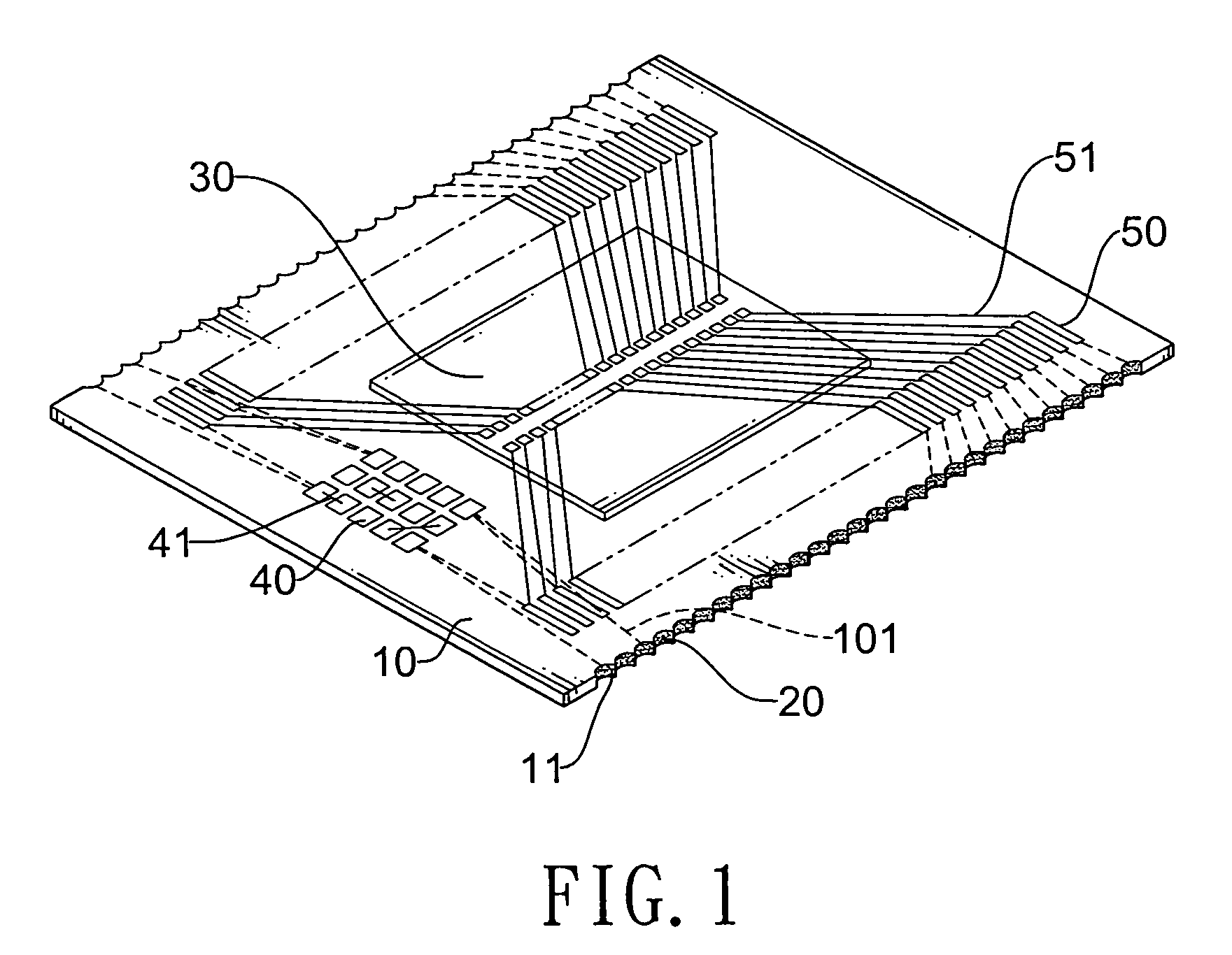
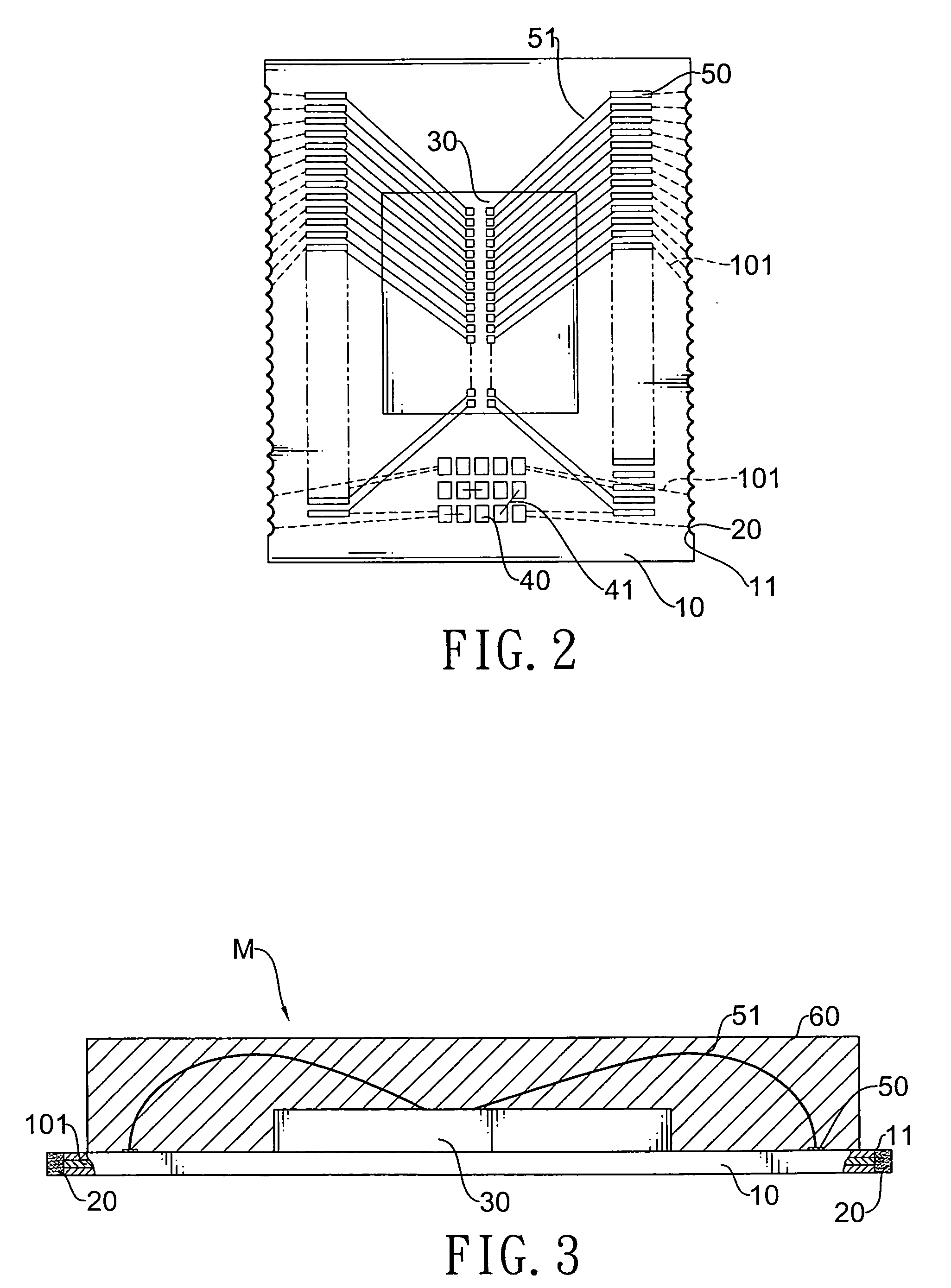
[0017]With reference to FIGS. 4 and 5, an insert card in accordance with the present invention may be a memory, a video graphics array (VGA) card or the like and comprises a motherboard (70) and at least one memory chip (M).

[0018]The motherboard (70) has a front surface, a rear surface, at least one chip region (71), multiple plugs (72), multiple chip contacts (73) and an optional connector (74).

[0019]The front surface of the motherboard (70) has two horizontal edges and two vertical edges.

[0020]The rear surface of the motherboard (70) has two horizontal edges.

[0021]The at least one chip region (71) has multiple edges and may be formed on the top or the rear surface of the motherboard (70). Furthermore, if the motherboard (70) has multiple chip regions (71), the chip regions (71) may be formed on both surfaces of the motherboard (70).

[0022]The plugs (72) are formed on the corresponding horizontal edges of the two surfaces on the motherboard (70).

[0023]The chip contacts (73) are form...


PUM


Abstract

A memory chip has a substrate, a die and an encapsulant. The substrate has multiple edges, a top surface, multiple die contacts, multiple outer contacts and multiple jumper contacts. The multiple die contacts are formed on the top surface of the substrate. The multiple outer contacts are formed on the edges of the substrate, and parts of the output contacts are electronically connected to parts of the die contacts directly. The multiple jumper contacts are formed on the top surface of the substrate and are electronically connected to the die contacts and outer contacts that are not connected together. The die is mounted on the substrate and electronically connects to the die contacts through bonding wires. The encapsulant is formed on the top surface of the substrate, entirely covers and protects the die contacts, the jumper contacts and the die.

Description

BACKGROUND OF THE INVENTION[0001]1. Field of the Invention[0002]The present invention relates to a memory chip and an insert card, and more particularly to a memory chip that can be controlled to change operating modes and an insert card having the memory chip thereon.[0003]2. Description of Related Art[0004]Computers are commonly used recently. The performance of the computers is based on hardwares in the computers, especially the insert cards such as memory, Video Graphics Array (VGA) card or the like.[0005]A conventional method to manufacture an insert card comprises steps of packaging memory chips and mounting the memory chips on a motherboard. The step of packaging memory chip comprises packaging multiple dies respectively to become multiple memory chips by quad flat package (QFP), small outline package (SOP), bump grid array (BGA) package or the like. The step of mounting the memory chips on a motherboard comprises installing the memory chips on a motherboard with welding poin...

Claims


Application Information

Patent Timeline
Patent Type & Authority Applications(United States)
IPC IPC(8): H05K7/00H01L23/49
CPCG11C5/06H01L23/49805H01L23/49838H01L2224/48227H01L2224/49171H01L24/49H01L24/48H01L2924/00H01L2224/05554H01L2924/00014H01L2924/10161H01L2924/181H01L2924/00012H01L2224/45099H01L2224/45015H01L2924/207
Inventor CHIH, CHING-SHUI
Owner KRETON CORP
Why Eureka
Try Eureka