
Method for reducing cross-talk induced source synchronous bus clock jitter

a synchronous bus clock and source technology, applied in the field of methods for reducing transition induced crosstalk edge jitter, to achieve the effect of reducing edge jitter and improving the eye diagram of received data

Inactive Publication Date: 2008-06-19
INT BUSINESS MASCH CORP
View PDF5 Cites 1 Cited by
  • Summary
  • Abstract
  • Description
  • Claims
  • Application Information

AI Technical Summary

Benefits of technology

[0012]Embodiments of the present invention purposely shift the propagating clock signal one-half clock cycle of the source clock that generates the data signal edges at each same polarity source clock edge. Thus the propagating clock is purposely shifted one-fourth of its clock cycle relative to the data signal edges. In this manner, noise coupled from propagating data signals to propagating clock signals only occur during either the logic one or logic zero clock state and not when the propagating clock is transitioning between logic states. When the propagating clock is received at the receiver chip, it is re-aligned with the data signals before it is used to sample the received data. The cross-talk induced jitter in the propagating clock is reduced resulting in higher reliability communication between IC chips.
[0014]A main clock of frequency F is used to launch data signals such that data transitions occur synchronous with the one edge of the source clock. A source clock with a frequency F / 2 is generated from the main clock. A propagating clock is coupled to an off-chip driver by clocking the source clock with the main clock such that the propagating clock is shifted one-half cycle of the main clock. The propagating clock has edge transitions that occur half way between data transitions of an alternating one / zero logic pattern. In this manner, any coupling between the propagating clock and an adjacent data signal will occur at static logic levels of either signal. Since coupling does not occur during edges of the propagating clock signal, its edge jitter is reduce thereby improving the eye diagram of received data clocked by the received propagating clock signal.

Problems solved by technology

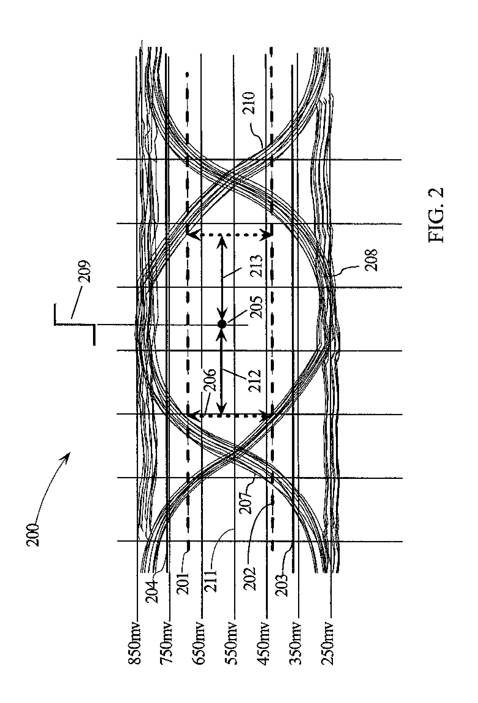
Since the data and clock edges are aligned, the coupled noise will affect edges of the clock signal resulting in the clock edges being shifted forward or backward depending whether the coupling occurs on a rising or falling edge of the data signal.

Method used


Image

  • Method for reducing cross-talk induced source synchronous bus clock jitter
  • Method for reducing cross-talk induced source synchronous bus clock jitter
  • Method for reducing cross-talk induced source synchronous bus clock jitter

Examples


Embodiment Construction

[0026]In the following description, numerous specific details are set forth to provide a thorough understanding of the present invention. However, it will be obvious to those skilled in the art that the present invention may be practiced without such specific details. In other instances, well-known circuits may be shown in block diagram form in order not to obscure the present invention in unnecessary detail. For the most part, details concerning timing considerations and the like have been omitted inasmuch as such details are not necessary to obtain a complete understanding of the present invention and are within the skills of persons of ordinary skill in the relevant art.

[0027]Refer now to the drawings wherein depicted elements are not necessarily shown to scale and wherein like or similar elements are designated by the same reference numeral through the several views.

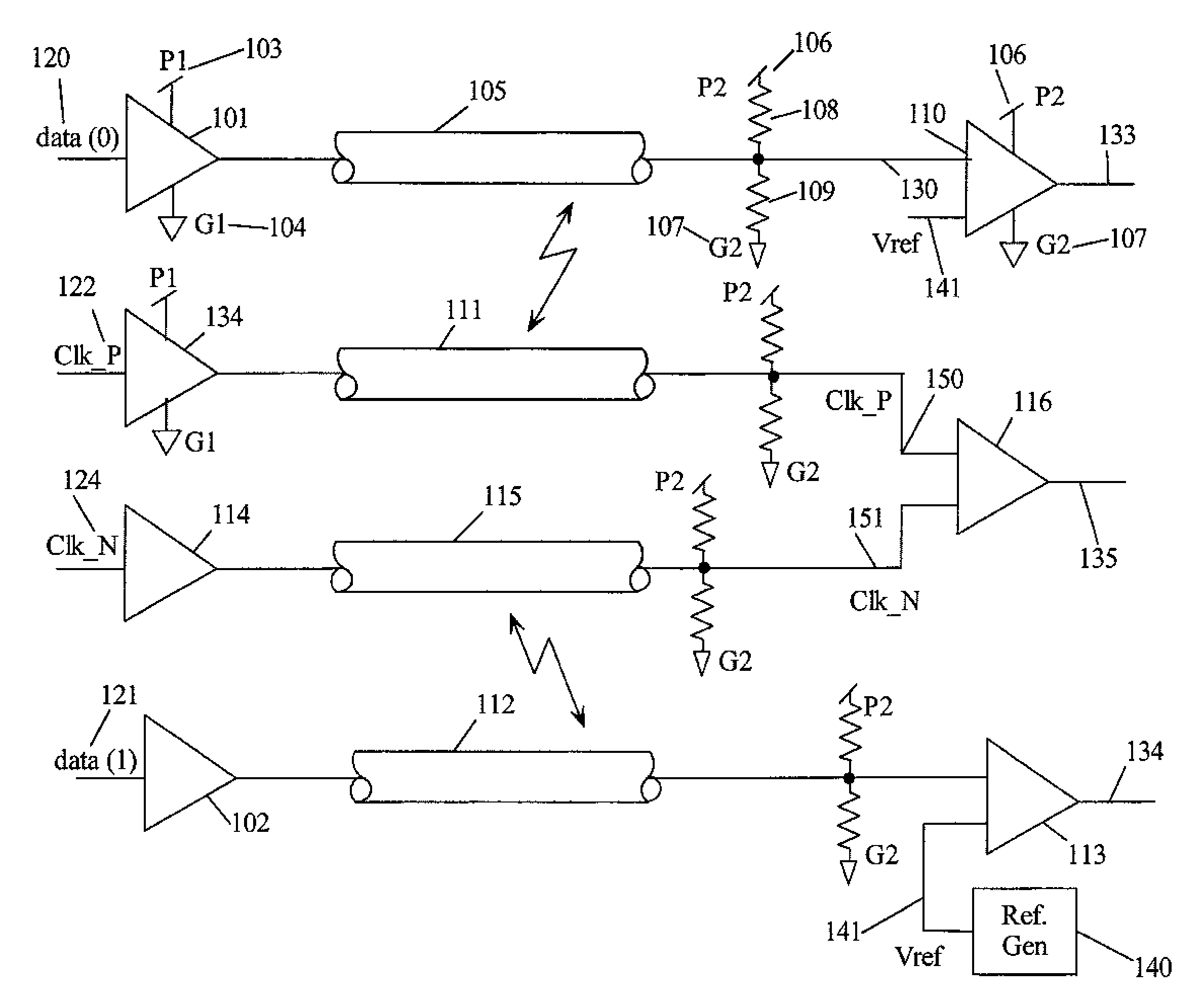
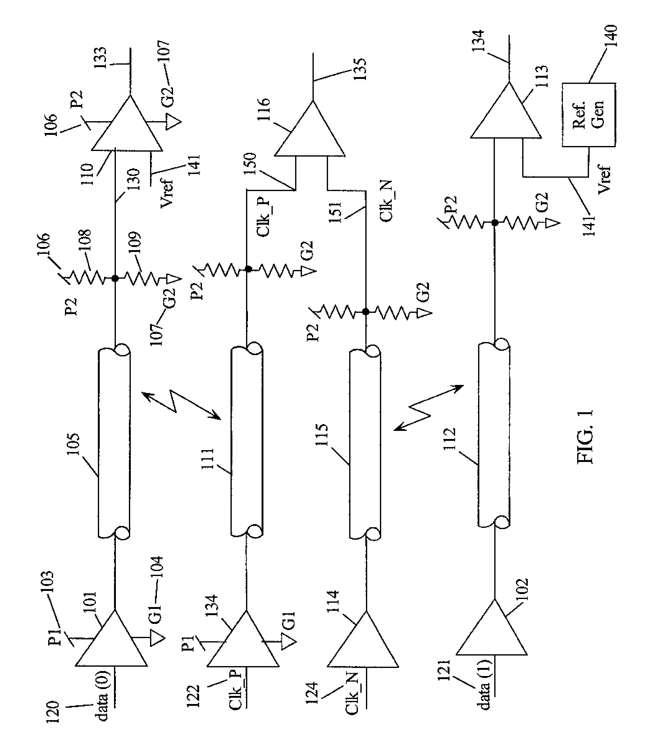
[0028]FIG. 1 is a circuit diagram of typical pseudo-differential signaling suitable for practicing embodiments of ...


PUM


Abstract

A first clock signal of frequency F is used to couple data to an off-chip driver (OCD) using a master / slave flip flop (FF), wherein the master latch is clocked with the first clock signal and the slave latch is clocked with the complement of the first clock signal. A second clock signal of frequency F / 2 is generated from the first clock signal. The second clock signal is shifted a time equal to substantially one-half the cycle of the first clock signal. In one embodiment, the second clock is shifted using a delay line circuit. In another embodiment, the second clock is shifted using a master / slave FF, wherein the master latch is clocked with the complement of the first clock signal and the slave latch is clocked with the first clock signal. The logic state transitions of the data between edges of the propagating clock thereby reducing coupling to the clock transitions and thus reducing edge jitter.

Description

TECHNICAL FIELD[0001]The present invention relates in general to off-chip transmission line drivers and receivers, and in particular, to methods for reducing transition induced cross-talk edge jitter in source synchronous clock systems.BACKGROUND INFORMATION[0002]Digital computer systems have a history of continually increasing the speed of the processors used in the system. As computer systems have migrated towards multiprocessor systems, sharing information between processors and memory systems has also generated a requirement for increased speed for the off-chip communication networks. Designers usually have more control over on-chip communication paths than for off-chip communication paths. Off-chip communication paths are longer, have higher noise, impedance mismatches, and have more discontinuities than on-chip communication paths. Since off-chip communication paths are of lower impedance, they require more current and thus more power to drive.[0003]When using inter-chip high-...

Claims


Application Information

Patent Timeline
Patent Type & Authority Applications(United States)
IPC IPC(8): H03K19/00H03K19/003
CPCH04L25/45
Inventor TRUONG, BAO G.DREPS, DANIEL MARKHARIDASS, ANANDSCHIFF, JOHN C.ZIEGELBEIN, JOEL D.
Owner INT BUSINESS MASCH CORP
Learn More