Probe and Probe Card

Inactive Publication Date: 2008-07-10
TOKYO ELECTRON LTD
View PDF8 Cites 5 Cited by
  • Summary
  • Abstract
  • Description
  • Claims
  • Application Information

AI Technical Summary

Benefits of technology

[0021]According to the present invention, a probe can be attached to a conta

Problems solved by technology

However, when each probe is joined to the contactor as in a conventional manner, it is necessary to join each probe by bringing a bonding tool for joining for example into contact with a joint portion of each of the probes, and thereby a long time is needed for joining all the probes to the contactor.
Also, it is necessary to use an apparatus for joining su

Method used


Image

  • Probe and Probe Card
  • Probe and Probe Card
  • Probe and Probe Card

Examples


Embodiment Construction

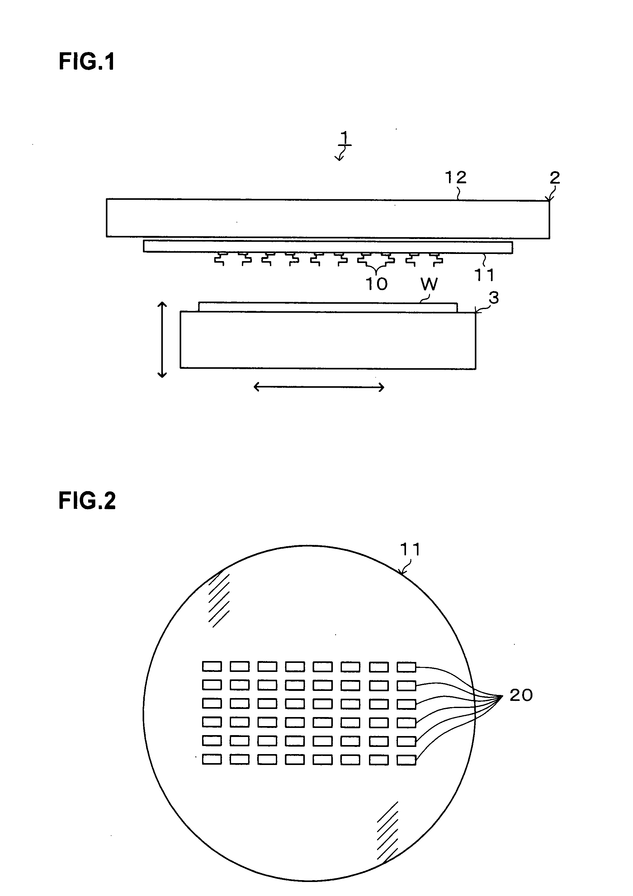
[0040]Hereinafter, a preferred embodiment of the present invention will be explained. FIG. 1 is an explanatory view of a vertical cross-section showing an overview of a structure of a probe apparatus 1.

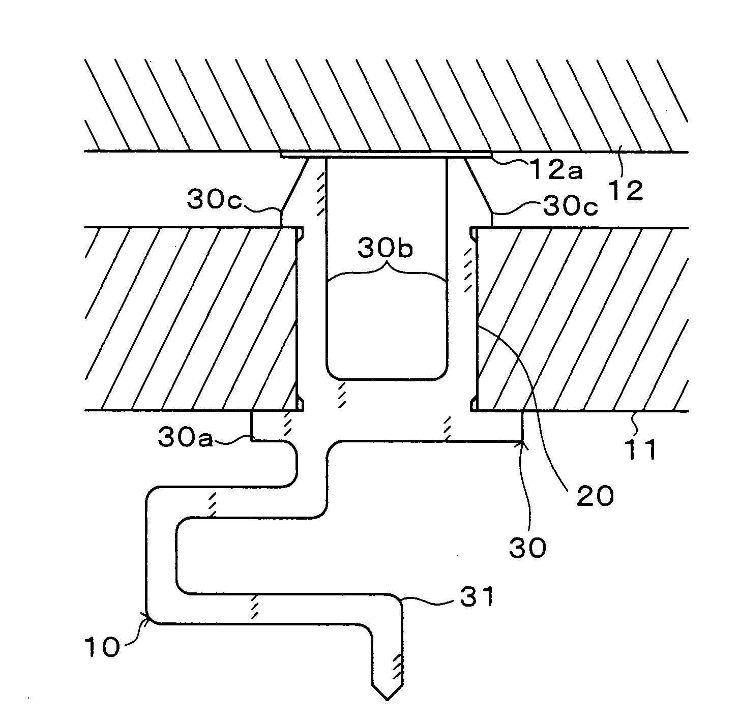
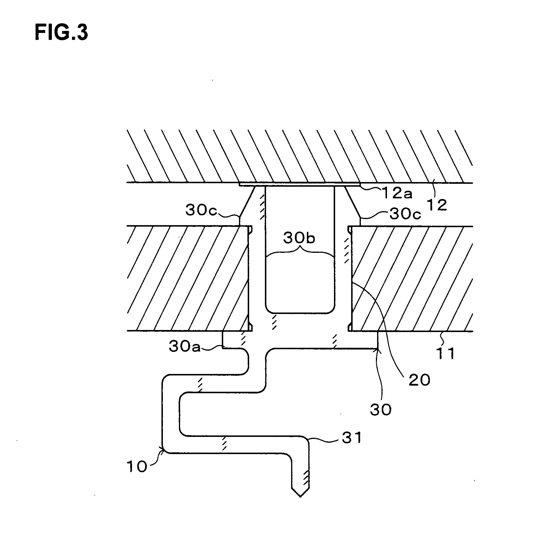
[0041]The probe apparatus 1 is provided with, for example, a probe card 2 and a mounting table 3 which mounts a wafer W as an object to be tested. The probe card 2 includes, for example, a contactor 11 as a support member supporting a plurality of probes 10 and a printed wiring board 12 as a circuit board for sending / receiving an electrical signal to / from the probes 10. The contactor 11 is provided so as to face the mounting table 3, and the printed wiring board 12 is provided on the contactor 11.

[0042]The contactor 11 is formed in a substantially disc shape for example, and on a central portion facing the wafer W on the mounting table 3, a plurality of through holes 20 are formed as shown in FIG. 2. Each through hole 20 is formed for example in a quadrangular shape in plan view. The ...


PUM


Abstract

An object of the present invention is to make it possible that a probe for testing electrical characteristics of an object to be tested is easily attached to a support member such as a contactor. A through hole is formed in the contactor. In the probe, a fitting/locking portion which can be fitted in this through hole is formed. The fitting/locking portion is formed to penetrate the through hole of the contactor and to be locked in the contactor in a state that a tip thereof is in contact with a connecting terminal of a printed wiring board. The fitting/locking portion itself is locked in the contactor by hooking a locking portion thereof to an end face on an upper side of the through hole.

Description

TECHNICAL FIELD[0001]The present invention relates to a probe and a probe card for testing electrical characteristics of an object to be tested.BACKGROUND ART [0002]Testing of electrical characteristics of an electronic circuit such as IC, LSI and the like formed on a semiconductor wafer for example is performed using a probe card attached to a probe apparatus. The probe card normally has a contactor which supports a large number of probes, and a circuit board connected electrically to the contactor. The contactor is arranged so that a lower face on which the probes are supported faces a wafer, and the circuit board is stacked and arranged on an upper face of the contactor. Testing of electrical characteristics of the wafer is performed by bringing the plurality of probes into contact with electrodes of the electronic circuit on the wafer, and applying an electrical signal for testing from the respective probes to the electrodes of the electronic circuit on the wafer via the circuit...

Claims


Application Information

Patent Timeline
IPC IPC(8): G01R31/02
CPCG01R1/06727G01R1/06716
Inventor TAKEKOSHI, KIYOSHI
Owner TOKYO ELECTRON LTD
Why Eureka
Try Eureka