Semiconductor memory device with ability to effectively adjust operation time for on-die termination

a memory device and semiconductor technology, applied in the field of semiconductor memory devices, can solve the problems of not meeting the operation speed required, more difficult to develop semiconductor memory devices, and difficult to implement synchronous semiconductor memory devices, and achieve the effect of effectively adjusting the operation time for on-die termination

Active Publication Date: 2008-07-10
SK HYNIX INC
View PDF10 Cites 31 Cited by
  • Summary
  • Abstract
  • Description
  • Claims
  • Application Information

AI Technical Summary

Benefits of technology

[0017]Embodiments of the present invention are directed to provide a semiconductor memory device with ability to effectively adjust operation time for on-die termination (ODT).

Problems solved by technology

However, in the development of the semiconductor IC until recent date, the data input / output speed between the data processing unit and the semiconductor memory device does not follow the operation speed required within the data processing unit.
However, since this synchronous memory device is not still sufficient for the operation speed of the data processing unit, DDR synchronous memory devices have been developed these days.
However, since the semiconductor memory device based on the high-speed DDR3 specification has the clock frequency of 800 MHz, 1066 MHz, 1333 MHz or 1600 MHz, it is more difficult to develop a semiconductor memory device in which the ODT timing parameter complies with the specification.
However, since the semiconductor memory device in the synchronous mode should operate in synchronization with the clock signals, it is not easy to implement the synchronous semiconductor memory device.
That is, in the case of tAON, tAOF and tADC parameters, the shorter the clock time tCK is, the more it is difficult to satisfy the specification.
The fluctuation of the ODT operation characteristics may be serious according to the processes of the semiconductor memory devices and it may be required to adjust the ODT timing whenever the semiconductor memory devices are manufactured.

Method used


Image

  • Semiconductor memory device with ability to effectively adjust operation time for on-die termination
  • Semiconductor memory device with ability to effectively adjust operation time for on-die termination
  • Semiconductor memory device with ability to effectively adjust operation time for on-die termination

Examples


Embodiment Construction

[0034]Hereinafter, a semiconductor memory device in accordance with the present invention will be described in detail referring to the accompanying drawings.

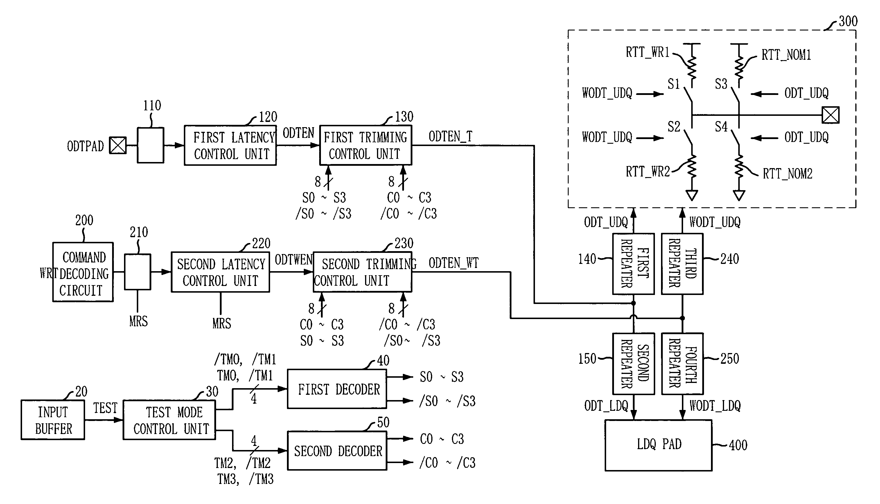
[0035]FIG. 4 is a block diagram illustrating a semiconductor memory device according to one embodiment of the present invention. Referring to FIG. 4, the semiconductor memory device according to one embodiment of the present invention includes an ODT command input buffer 110 associated with ODT operations, a first latency control unit 120, a first trimming control unit 130, a first repeater 140, a second repeater 150, a command decoding circuit 200 associated with a dynamic ODT operations, a write command input buffer 210, a second latency control unit 220, a second trimming control unit 230, a third repeater 240 and a fourth repeater 250. Also, the semiconductor memory device includes a UDQ pad region 300 and a LDQ pad region 400. Further, the semiconductor memory device includes an input buffer 20, a test mode control unit 30,...


PUM


Abstract

A semiconductor memory device is effectively able to adjust operation time for on-die termination (ODT). The semiconductor memory device includes a latency control unit, a control signal generating unit, a trimming control unit, and a termination circuit. The latency control unit produces an ODT driving enable signal by delaying an ODT operation signal from an external circuit during a predetermined latency. The control signal generating unit produces control signals to control a change of waveform of the ODT driving enable signal. The trimming control unit changes the waveform of the ODT driving enable signal in response to the control signals, thereby outputting a ODT driving signal. The termination circuit connects a termination resistance to an impedance adjusting node in response to the ODT driving signal.

Description

CROSS-REFERENCE TO RELATED APPLICATIONS[0001]The present invention claims priority of Korean patent application no. 10-2007-0002893, filed in the Korean Patent Office on Jan. 10, 2007, which is incorporated by reference in its entirety.BACKGROUND OF THE INVENTION[0002]The present invention relates to a semiconductor memory device; and, more particularly, to a circuit performing an ODT (on-die termination) operation in a semiconductor memory device.[0003]In a system having different semiconductor devices which perform various functions, a semiconductor memory device is used as an apparatus for storing data. The semiconductor memory device outputs data, which are correspondent to address inputted from data processing unit to request for the data, for example, a central processing unit and stores in a unit cell the data which are delivered from the data processing unit based on the corresponding address.[0004]As the operation speed of the system becomes higher, the data input / output sp...

Claims


Application Information

Patent Timeline
Patent Type & Authority Applications(United States)
IPC IPC(8): H03K19/0175
CPCG11C5/063G11C7/1051H04L25/0264G11C7/22G11C2207/2272G11C7/1057H03K19/0005G11C2207/2254
Inventor KIM, KYUNG-WHAN
Owner SK HYNIX INC
Why Eureka
Try Eureka