High Density Interconnection Device With Dielectric Coating

a dielectric coating and high density technology, applied in the direction of coupling devices, two-part coupling devices, electrical devices, etc., can solve the problem of bulky spacers, and achieve the effect of reducing or minimizing inter-wafer electrical interferen

Inactive Publication Date: 2008-07-17
INTERPLEX IND
View PDF9 Cites 1 Cited by
  • Summary
  • Abstract
  • Description
  • Claims
  • Application Information

AI Technical Summary

Benefits of technology

[0007]A dielectric coating is applied to at least one body surface of one or more of the wafers to prevent electrical bridging between the adjacent signal and shield wafers, e.g., when conductive debris is lodged between the wafers. The thickness of the dielectric coating can generally range from about 0.0001″ (0.0025 mm) to about 0.06″ (1.5 mm). The dielectric coating can also be used to eliminate or minimize inter-wafer electrical interference.

Problems solved by technology

These spacers are bulky, are used only to separate adjacent terminal sets, and are not provided in the body of the connector.

Method used


Image

  • High Density Interconnection Device With Dielectric Coating
  • High Density Interconnection Device With Dielectric Coating
  • High Density Interconnection Device With Dielectric Coating

Examples


Embodiment Construction

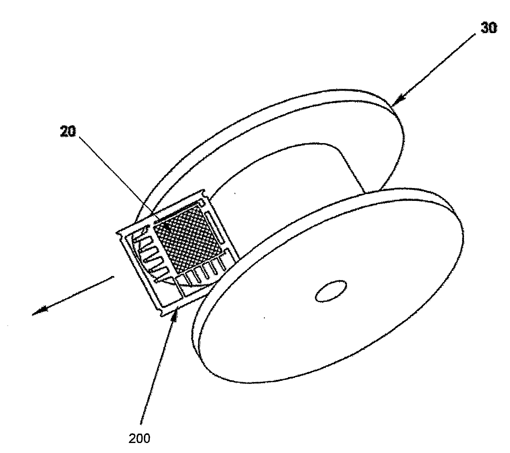
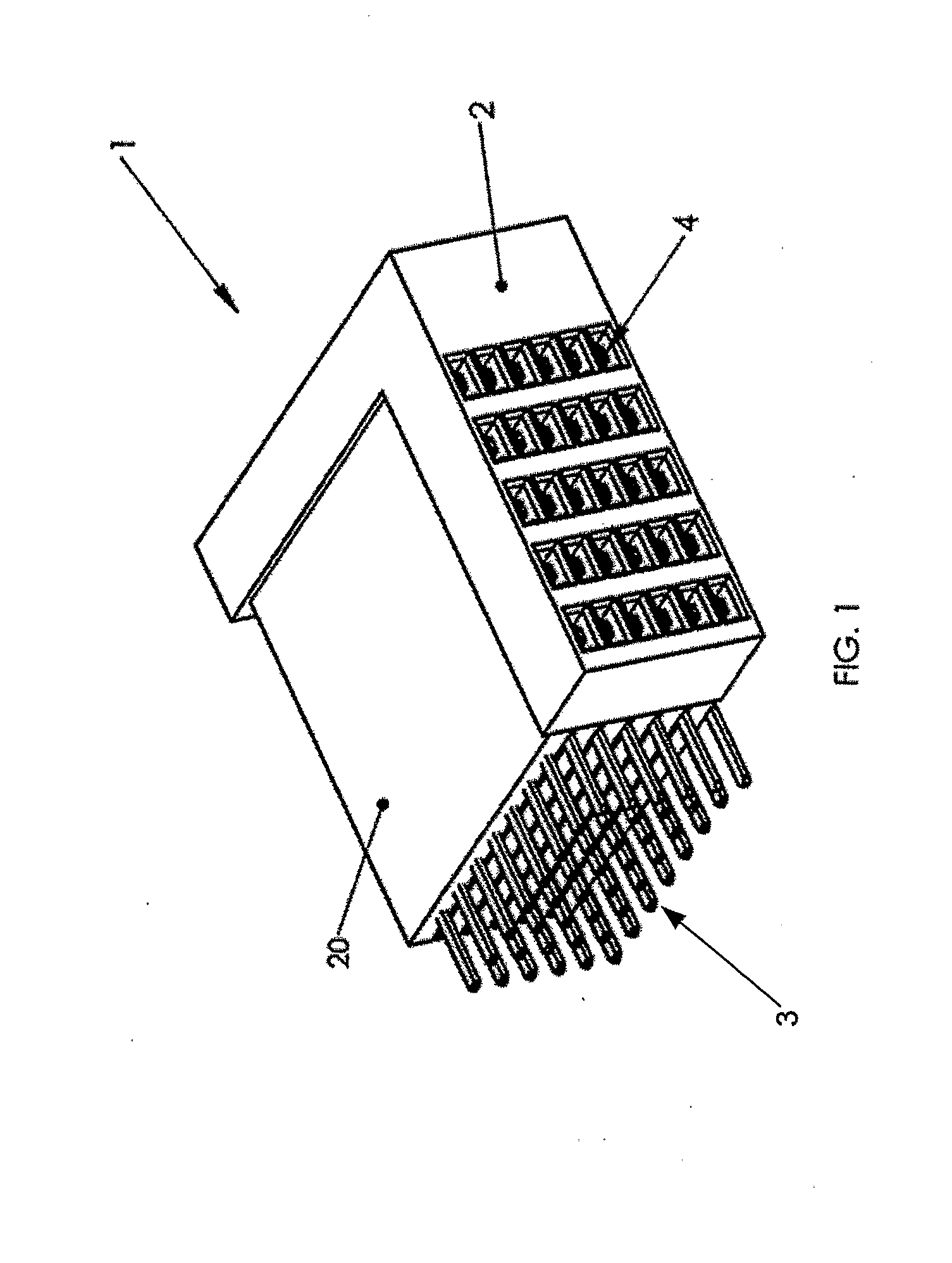
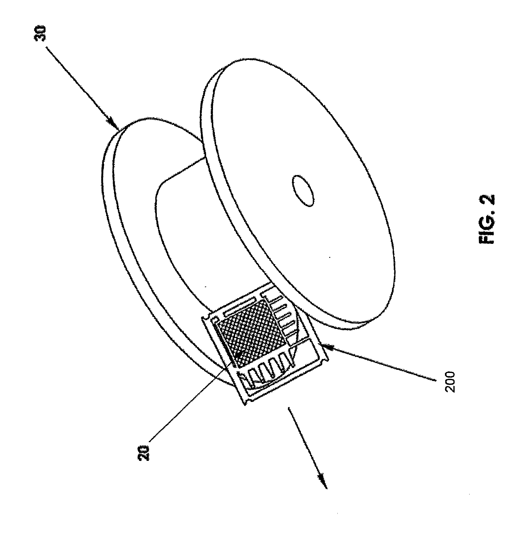
[0016]FIG. 1 illustrates a high density interconnection device, or connector 1, in accordance with an embodiment of the present invention, which is used to connect two circuit boards (not shown) together via a mating connector (not shown). One of the two connectors is a “plug” connector and the other is a “receptacle” connector. The connector shown in FIG. 1 is termed the receptacle connector because it receives the plug connector. It is to be understood that the plug connector is formed using a similar method that is used to form the receptacle connector as described herein.

[0017]The connector 1 has a housing 2, a mounting portion 3, and a mating portion 4. The housing 2 can be a molded or extruded plastic housing. The mounting portion 3 can include solder legs or connector leads that mount or are wave soldered to the circuit board. The mating portion 4 can include receptacle contacts that are stitched or inserted into holes of the housing 2 to mate with a mating portion of the plu...


PUM

PropertyMeasurementUnit
densityaaaaaaaaaa
dielectricaaaaaaaaaa
conductiveaaaaaaaaaa

Abstract

A high-density interconnection device or connector (1) that is formed with wafer in a stacked arrangement. The stack of wafers (20) is arranged to include signal wafers (20b) that alternate with shield wafers (20a). A dielectric coating (40) is applied to at least one body surface of one or more of the wafer to prevent electrical bridging between the adjacent signal and shield wafers (20a, 20b), e.g. when conductive debris is lodged between the wafers (20).

Description

TECHNICAL FIELD[0001]The present invention relates generally to high density interconnection devices and more specifically to a high density interconnection device provided with a dielectric coating.BACKGROUND[0002]It is known to use dielectric spacers in high density connector assemblies to provide insulation between terminals. U.S. Pat. No. 6,805,587 to Hazelton et al., the contents of which are incorporated herein by reference, discloses a dielectric spacer disposed on the terminals of a high density connector assembly. The connector assembly connects two circuit boards using mating connectors, such as a plug connector connected to one circuit board and a receptacle connector connected to the other circuit board. Each of the connectors includes a plurality of conductive terminals arranged in distinct sets for mating with corresponding terminals of the mating connector. Each set of terminals is separated by a discrete dielectric spacer so that each spacer insulates each set of ter...

Claims


Application Information

Patent Timeline
Patent Type & Authority Applications(United States)
IPC IPC(8): H01R24/00
CPCH01R13/405Y10T29/49002H01R23/688H01R13/514H01R13/6471H01R13/6586H01R13/6599H01R12/00
Inventor THOMAS, RALPHFRECHETTE, RAYMOND A.
Owner INTERPLEX IND
Why Eureka
Try Eureka