
Method and device for improving debug time of a display apparatus

a display apparatus and debug time technology, applied in the field of debug methods and devices for improving debug time of display apparatuses, to achieve the effect of saving tim

Inactive Publication Date: 2008-07-24
NOVATEK MICROELECTRONICS CORP
View PDF3 Cites 7 Cited by
  • Summary
  • Abstract
  • Description
  • Claims
  • Application Information

AI Technical Summary

Benefits of technology

[0011]Accordingly, the present invention is directed to a method and a device for improving debug time of a display apparatus, which are adapted for increasing reading / writing speed and reducing the cost.
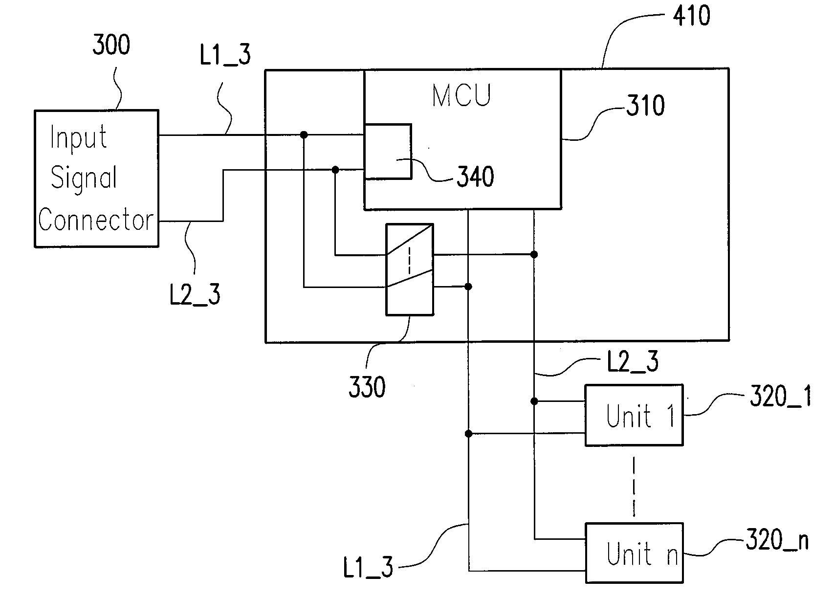
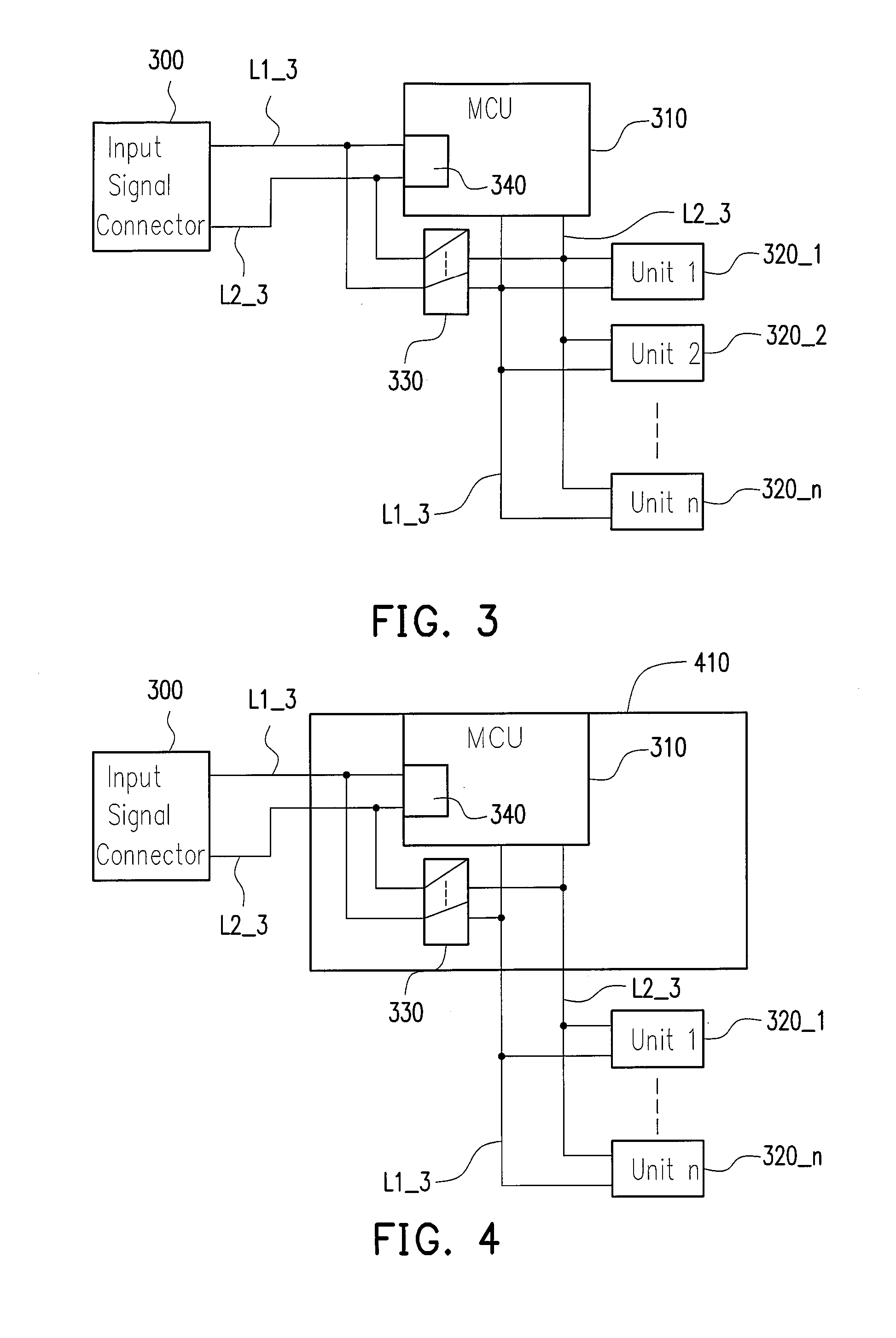
[0014]The present invention is directed to a switch, such that when entering the debug mode, the MCU outputs a signal to command the switch to switch to directly connect the input signal connector and the units via the IIC bus. Therefore, the debug process would not be processed by the MCU. As such, states between the units can be judged at once, and failures can be found by directly debugging without requiring taking off the housing and shutting off the power supply, thus saving time.

Problems solved by technology

As such, states between the units can be judged at once, and failures can be found by directly debugging without requiring taking off the housing and shutting off the power supply, thus saving time.

Method used


Image

  • Method and device for improving debug time of a display apparatus
  • Method and device for improving debug time of a display apparatus
  • Method and device for improving debug time of a display apparatus

Examples


Embodiment Construction

[0023]Reference will now be made in detail to the present preferred embodiments of the invention, examples of which are illustrated in the accompanying drawings. Wherever possible, the same reference numbers are used in the drawings and the description to refer to the same or like parts.

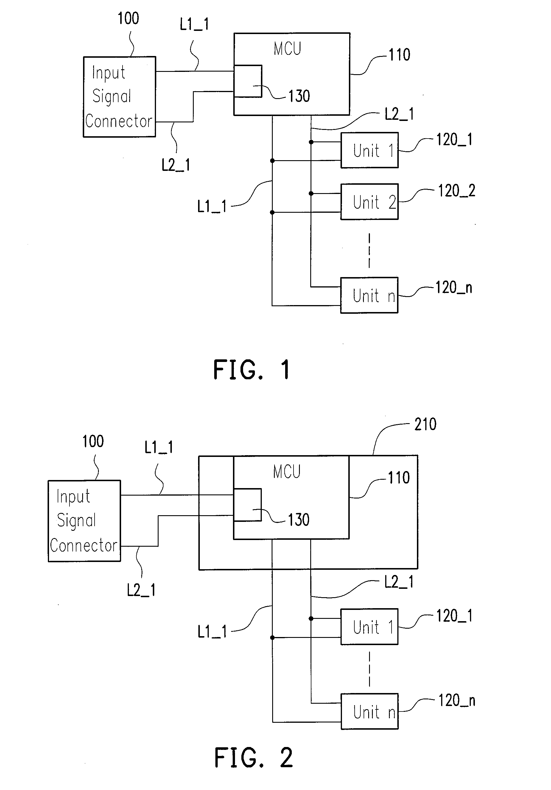
[0024]As discussed above, in the aforementioned conventional debug method for display apparatus, reading / writing control operations between the debug tool and the devices must be transmitted via the MCU and sent from the MCU to control the IIC devices to read / write. However, more devices controlled by the MCU require more program space reserved in the MCU, thus increasing the production cost. Accordingly, with respect to the foregoing shortcomings, the present invention provides a method without adding much program space of the MCU and / or amending the debug tool program. The method includes employing an external switch for switching DDC IIC channel to an ordinary IIC bus under a debug mode and contro...


PUM


Abstract

A method and a device for improving debug time of a display apparatus are provided. The display apparatus includes an input signal connector for receiving an external input signal, an MCU, a bus and a plurality of units. The input signal connector is connected to the MCU via the bus, and the MCU is connected to the plurality of units via the bus. First, whether the MCU has entered the debug mode is detected; and when it is detected that the MCU has entered the debug mode, the bus switches to directly connect to the plurality of units in the display apparatus for allowing the external signal transmitted directly to the plurality of units for debugging.

Description

CROSS-REFERENCE TO RELATED APPLICATION[0001]This application claims the priority benefit of Taiwan application serial no. 96102040, filed Jan. 19, 2007. All disclosure of the Taiwan application is incorporated herein by reference.BACKGROUND OF THE INVENTION[0002]1. Field of the Invention[0003]The present invention generally relates to a debug method and a device for a display apparatus, and more particularly to a method and a device for improving debug time of a display apparatus.[0004]2. Description of Related Art[0005]Generally, during fabrication, assembling, or burn-in test of various displays, failures often occur. However, at this stage, since the display has already be installed, the housing thereof has to be taken off in order to find out the true reason that causes the problem. Unfortunately, the phenomenon of failure is often not likely to be favourably simulated, which often delays production or testing plan thereof.[0006]Generally, a display includes at least one externa...

Claims


Application Information

Patent Timeline
Patent Type & Authority Applications(United States)
IPC IPC(8): G06F9/44
CPCG06F11/2221
Inventor LIU, MING-CHANGCHEN, KUO-CHI
Owner NOVATEK MICROELECTRONICS CORP
Learn More