

Wiring structure, forming method of the same and printed wiring board
a multi-layer printed wiring and wiring board technology, applied in the direction of printed circuit aspects, conductive pattern formation, semiconductor/solid-state device details, etc., can solve the problems of insufficient connection between them, difficult to maintain sufficient high and the reliability of the wiring board or the wiring board can be improved, and the effect of effective forming a wiring structur
- Summary
- Abstract
- Description
- Claims
- Application Information
AI Technical Summary
Benefits of technology
Problems solved by technology
Method used
Image

Examples
Embodiment Construction
[0055]An embodiment of the present invention will hereinafter be described in detail. It is to be noted that in the drawings, the same element is denoted with the same reference numeral, and redundant description is omitted. Moreover, it is assumed that upper, lower, left and right positional relations are based on a positional relation shown in the drawing, unless specified otherwise. Furthermore, a dimensional ratio of the drawing is not limited to a shown ratio. The following embodiment is an illustration for the description of the present invention, and it is not intended that the present invention is limited only to the embodiment. Furthermore, the present invention can variously be modified without departing from the scope thereof.
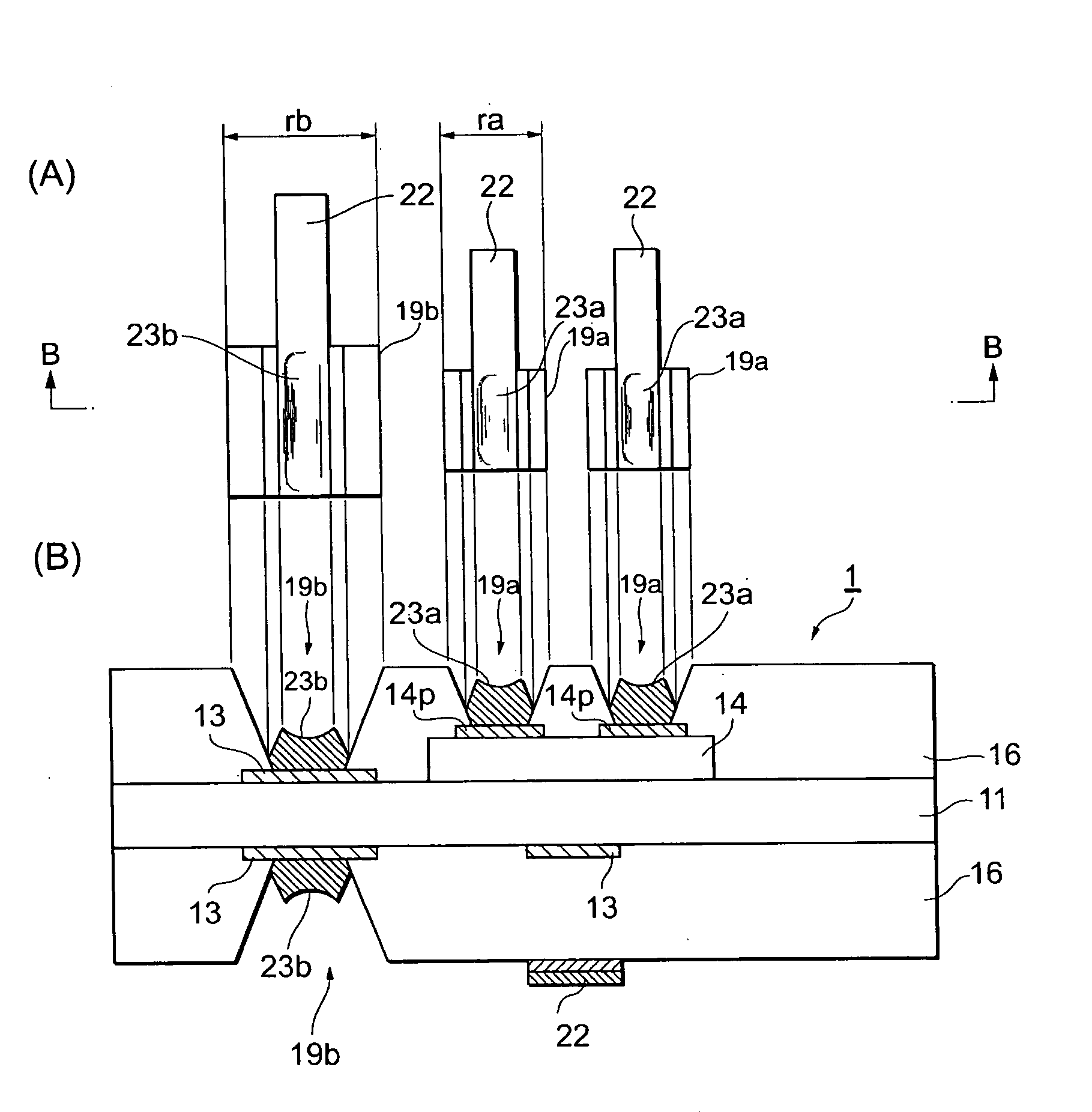
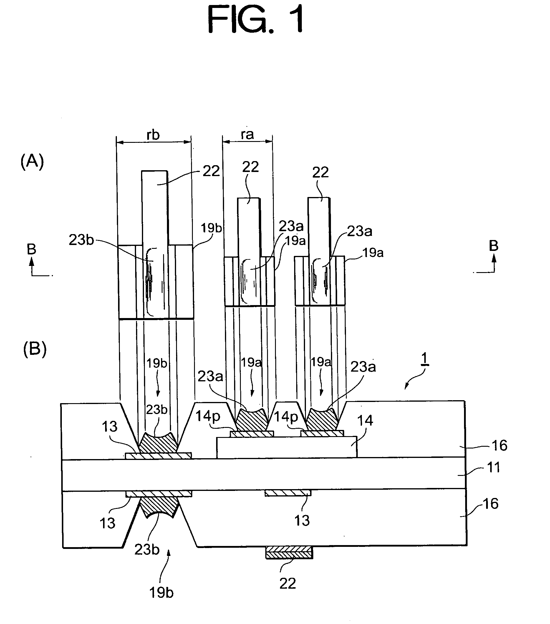
[0056]FIG. 1A is a plan view showing an outline of a main part of one example of a semiconductor-embedded substrate including one preferable embodiment of the wiring structure according to the present invention, and FIG. 1B is a sectional view cut al...
PUM
| Property | Measurement | Unit |
|---|---|---|
| thickness | aaaaa | aaaaa |
| height | aaaaa | aaaaa |
| width diameter | aaaaa | aaaaa |
Abstract
Description
Claims
Application Information