

Integrated rotation rate and acceleration sensor and method for manufacturing an integrated rotation rate and acceleration sensor
a technology of rotation rate and acceleration sensor and integrated technology, which is applied in the direction of acceleration measurement using interia force, turn-sensitive devices, instruments, etc., can solve the problems of increasing the cost of the micromechanical device, reducing the signal-to-noise ratio, and reducing the use of additional getter materials, so as to improve the connection properties, increase the melting temperature, weaken or shift the effect of alge connection
- Summary
- Abstract
- Description
- Claims
- Application Information
AI Technical Summary
Benefits of technology
Problems solved by technology
Method used
Image

Examples
Embodiment Construction
[0029]In the various figures, identical parts are always provided with identical reference numerals and are therefore generally also only cited or mentioned once in each case.
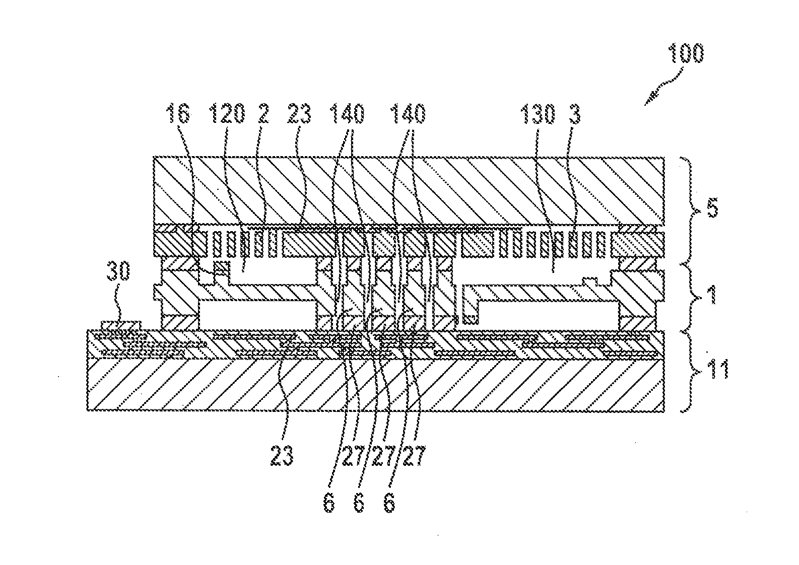
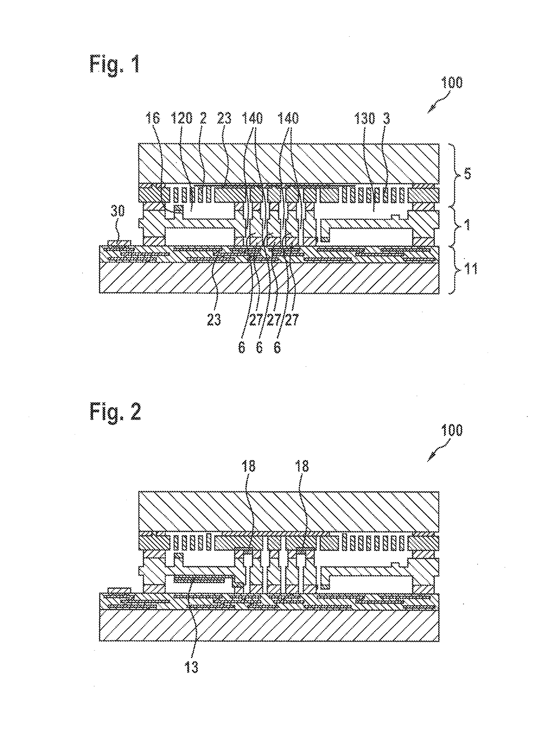
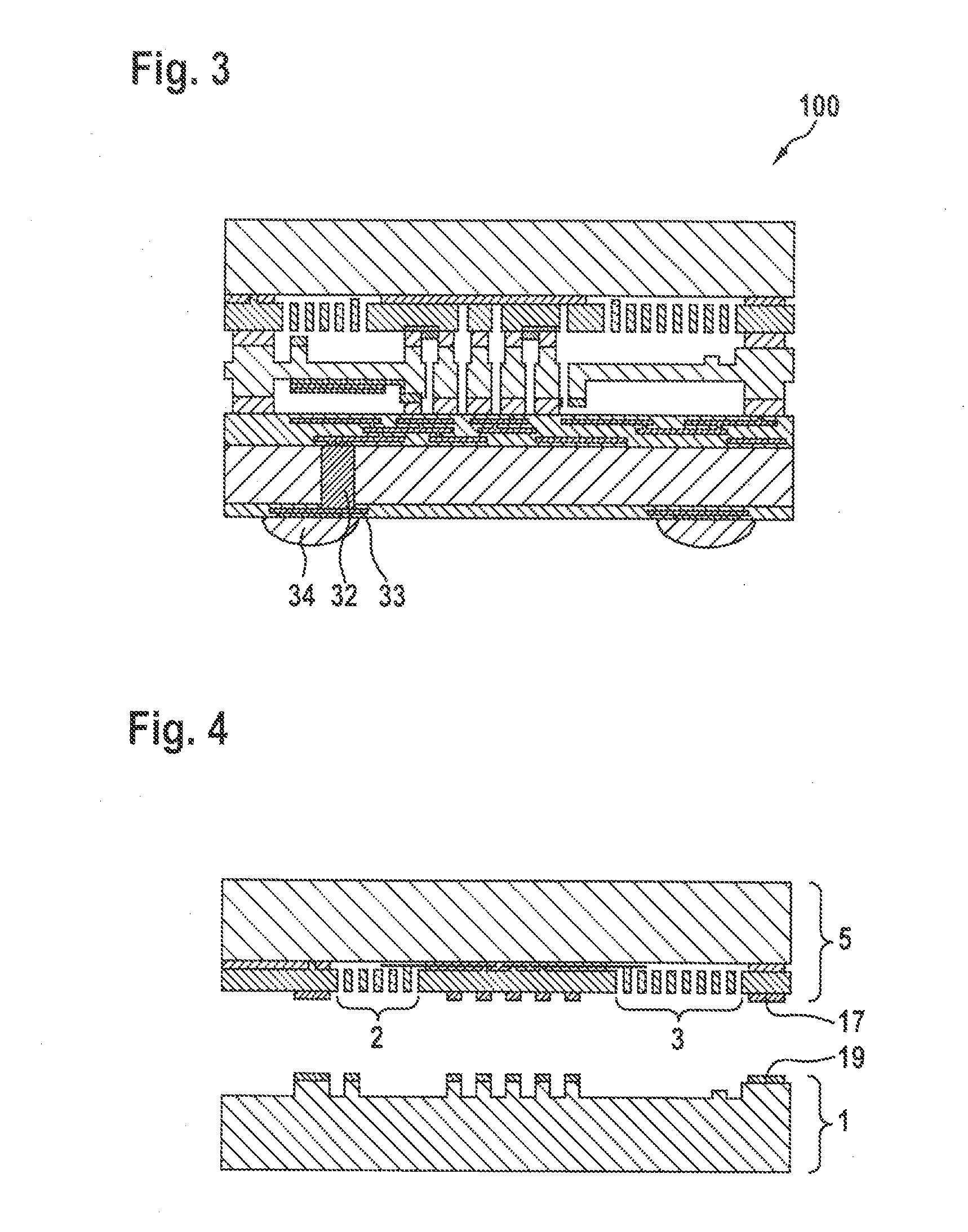
[0030]FIG. 1 shows a first specific embodiment according to the present invention of a micromechanical device 100. It includes an intermediate wafer 1, an evaluation wafer 11, and a sensor wafer 5, which have a shared main plane of extension and are stacked in such a way that intermediate wafer 1 is situated between evaluation wafer 11 and sensor wafer 5. In the specific embodiment shown, a first sensor element 2 and a second sensor element 3 are part of sensor wafer 5. First sensor element 2 and second sensor element 3 are preferably seismic masses, which are each part of a sensor system, such a micromechanical device 100 being able to include a plurality of (in this specific embodiment two) sensor elements 3. In particular, first sensor element 2 is part of an acceleration sensor and second sensor element 3 i...
PUM
| Property | Measurement | Unit |
|---|---|---|
| angle | aaaaa | aaaaa |
| gas pressure | aaaaa | aaaaa |
| electrically conductive | aaaaa | aaaaa |
Abstract
Description
Claims
Application Information