

Lateral mosfet and manufacturing method thereof
a technology of mosfet and lateral mosfet, which is applied in the direction of basic electric elements, electrical apparatus, and semiconductor devices, can solve the problems of large difference between two incident angles, ineffective use of channel ch in the depth direction, and inability to effectively contribute to the flow of electrons, etc., and achieves the effect of wide channel width and decreasing resistan
- Summary
- Abstract
- Description
- Claims
- Application Information
AI Technical Summary
Benefits of technology
Problems solved by technology
Method used
Image

Examples
embodiments
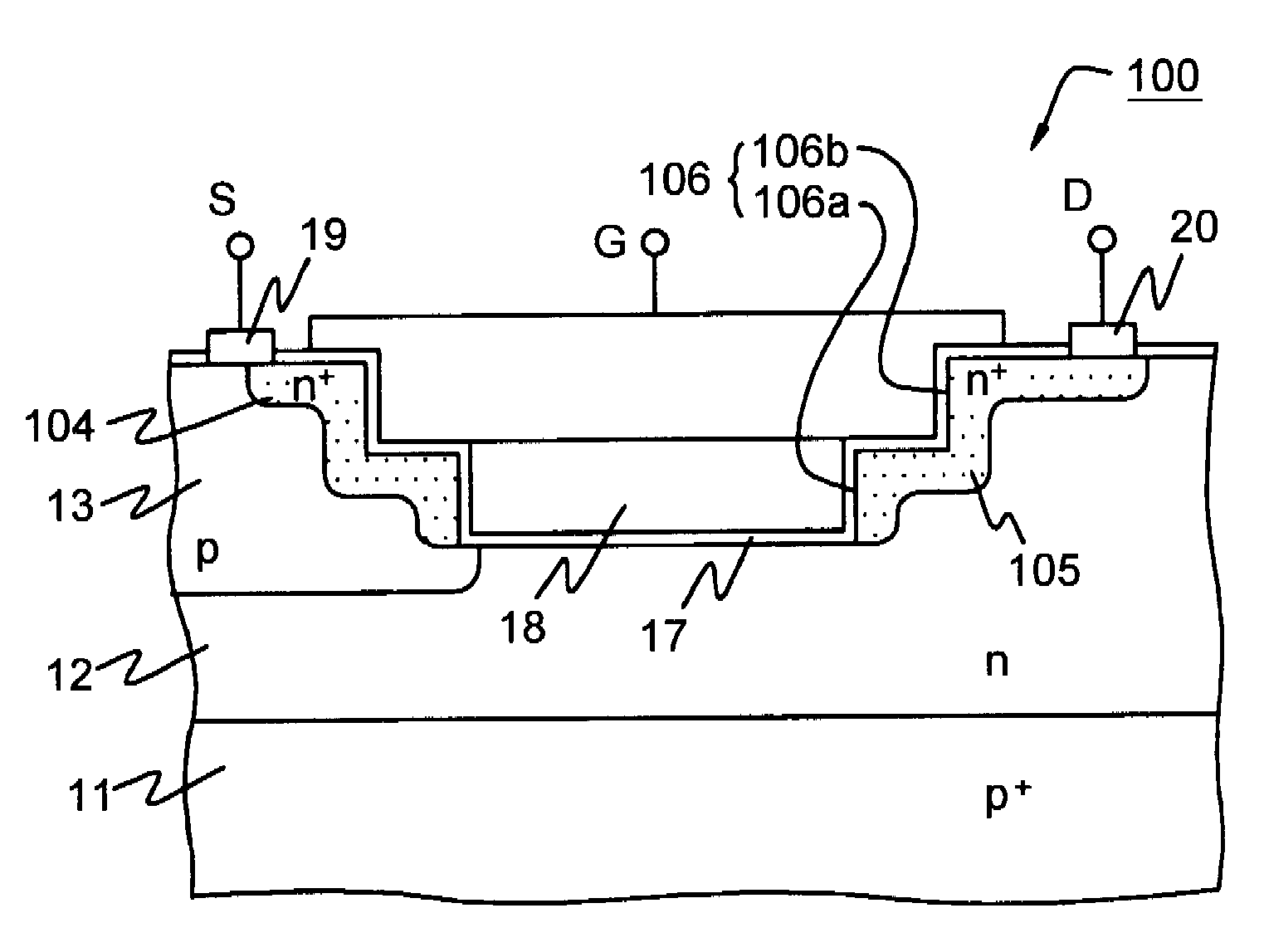
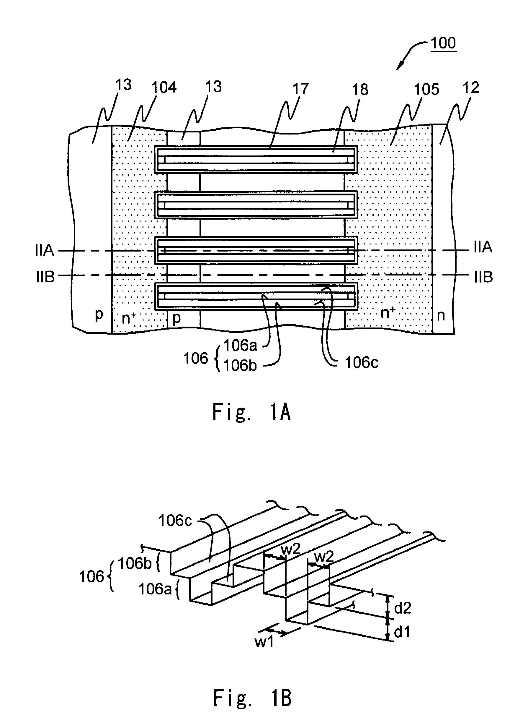
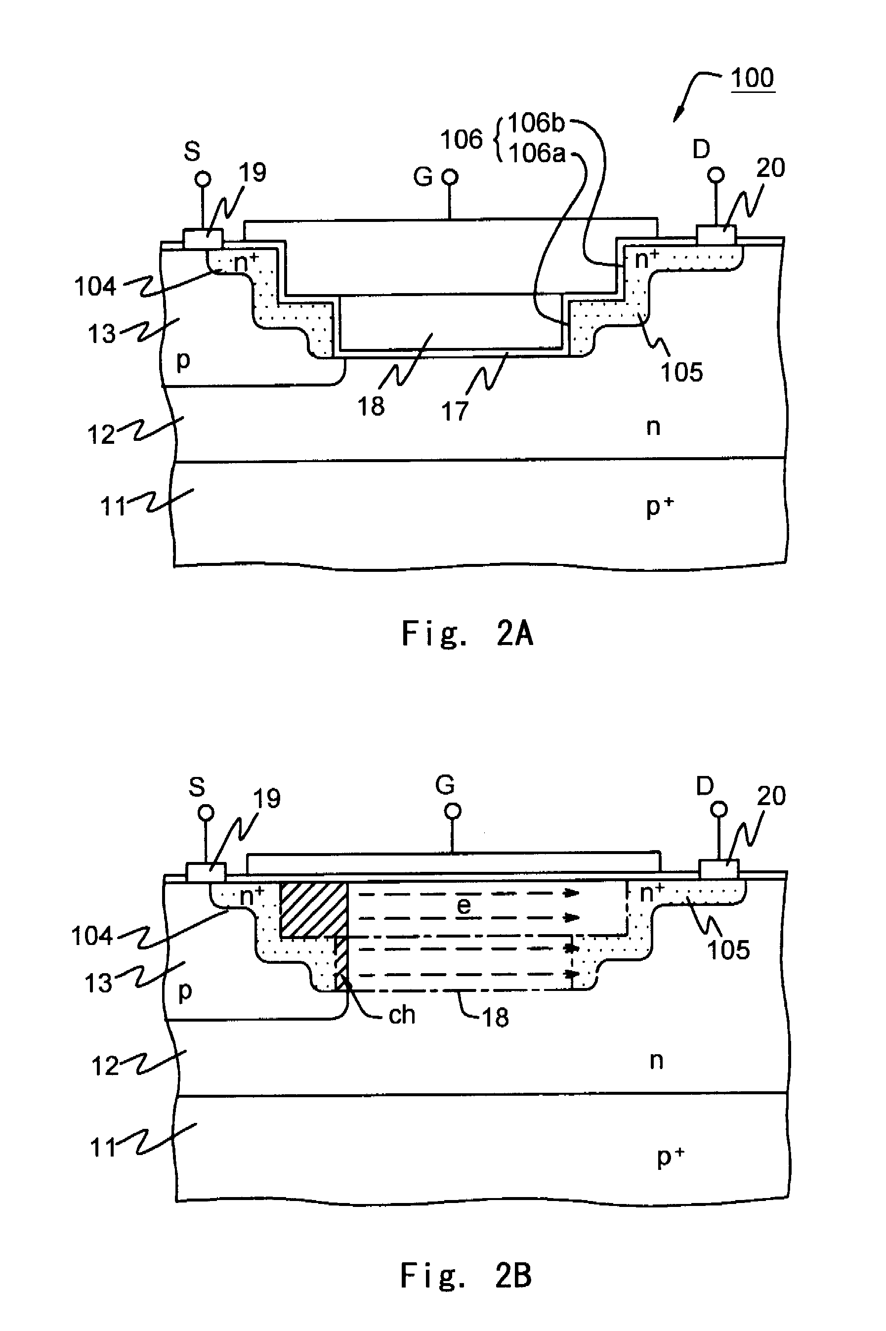
[0049]A structure of one example of the lateral MOSFET having a trench gate structure of the present invention is shown in FIGS. 1A, 1B, 2A, 2B, and 4. Note that the same reference symbols are given to the parts identical to FIGS. 7A, 7B, 8A, and 8B.
[0050]FIG. 1A is a plan view and FIG. 1B is a perspective view showing a trench shape. FIG. 2A is a cross sectional view taken along the line IIA-IIA in FIG. 1A. FIG. 2B is a cross sectional view taken along the line IIB-IIB in FIG. 1A. FIG. 4 is a cross sectional view of the trench portion. FIG. 1A does not include a surface electrode.
[0051]In FIGS. 1A, 1B, 2A, and 2B, the lateral MOSFET 100 has a p-type substrate 11, an n-type high-resistance layer 12, a p-type well layer 13, an n-type source layer 104, an n-type drain layer 105, a trench 106, a lower trench 106a, an upper trench 106b, 106c is a step surface, a gate insulation film 17, a gate electrode 18, a source electrode 19, and a drain electrode 20. Here, w1 is a lower trench widt...
PUM
 Abstract
Description
Claims
Application Information