STRUCTURE AND METHOD FOR COMPACT LONG-CHANNEL FETs

a long-channel fet and compact technology, applied in the field of structure and method of long-channel fets, can solve the problems of reducing the channel length of a transistor and increasing the short-channel effect, and the general difficulty of fabricating long-channel fets into a compact structure, and achieves the effect of wide channel width and long channel length

Inactive Publication Date: 2009-05-14
IBM CORP
View PDF11 Cites 8 Cited by
  • Summary
  • Abstract
  • Description
  • Claims
  • Application Information

AI Technical Summary

Benefits of technology

[0007]The present invention provides a compact semiconductor structure including at least one field effect transistor (FET) located upon and within a surface of a semiconductor substrate in which the at least one FET includes a long channel length and / or a wide channel width.

Problems solved by technology

However, reducing the channel length of a transistor also increases short-channel effects.
However, long channel FETs are generally difficult to fabricate into a compact structure since long channel FETs are restricted by the contact pitch.

Method used


Image

  • STRUCTURE AND METHOD FOR COMPACT LONG-CHANNEL FETs
  • STRUCTURE AND METHOD FOR COMPACT LONG-CHANNEL FETs
  • STRUCTURE AND METHOD FOR COMPACT LONG-CHANNEL FETs

Examples


Embodiment Construction

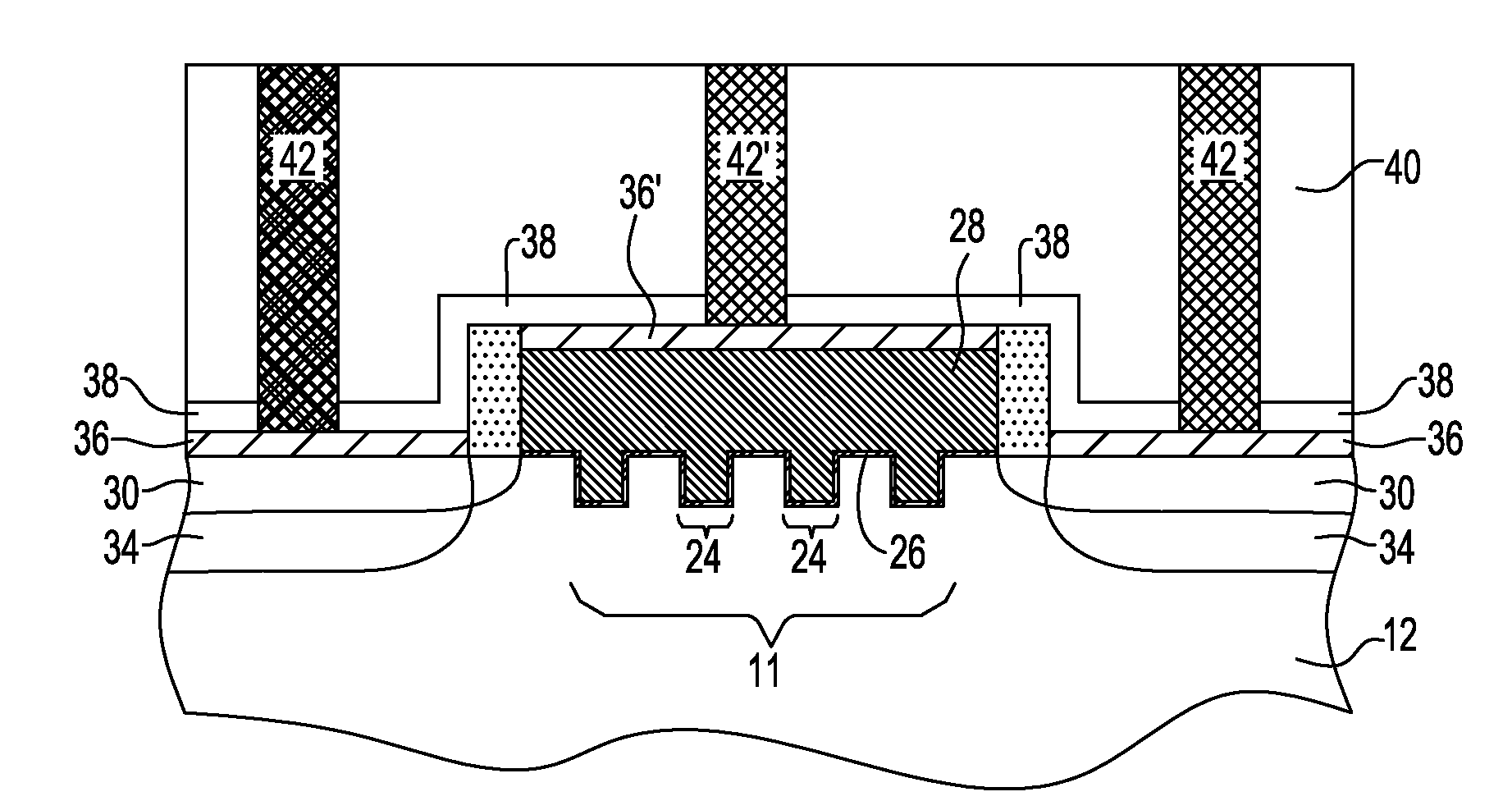
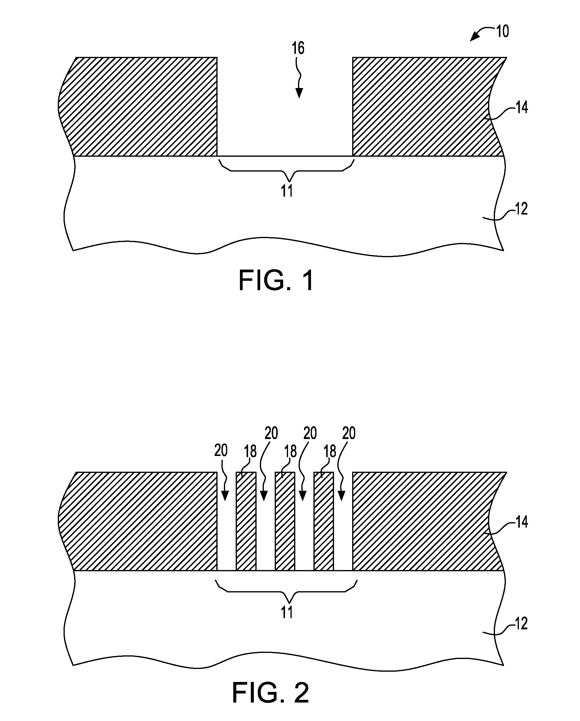
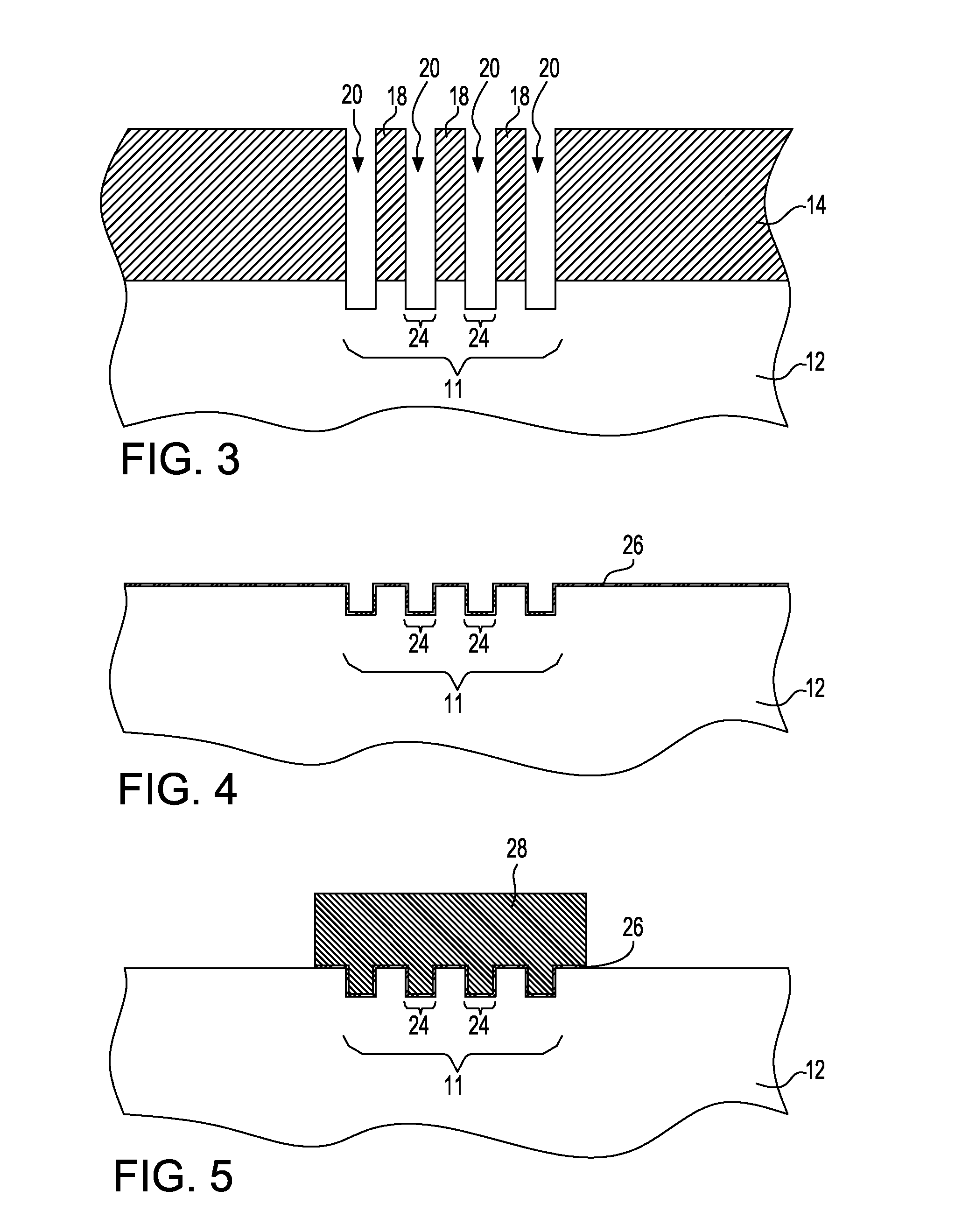
[0025]The present invention, which provides a semiconductor structure including a compact FET having a long channel length and / or wide-channel width as well as a method of fabricating the same, will now be described in greater detail by referring to the following description and drawings that accompany the present application. It is noted that the drawings of the present application are provided for illustrative purposes and, as such, they are not drawn to scale.

[0026]In the following description, numerous specific details are set forth, such as particular structures, components, materials, dimensions, processing steps and techniques, in order to provide a thorough understanding of the present invention. However, it will be appreciated by one of ordinary skill in the art that the invention may be practiced without these specific details. In other instances, well-known structures or processing steps have not been described in detail in order to avoid obscuring the invention.

[0027]It ...


PUM


Abstract

A compact semiconductor structure including at least one FET located upon and within a surface of a semiconductor substrate in which the at least one FET includes a long channel length and/or a wide channel width and a method of fabricating the same are provided. In some embodiments, the ordered, nanosized pattern is oriented in a direction that is perpendicular to the current flow. In such an embodiment, the FET has a long channel length. In other embodiments, the ordered, nanosized pattern is oriented in a direction that is parallel to that of the current flow. In such an embodiment, the FET has a wide channel width. In yet another embodiment, one ordered, nanosized pattern is oriented in a direction perpendicular to the current flow, while another ordered, nanosized pattern is oriented in a direction parallel to the current flow. In such an embodiment, a FET having a long channel length and wide channel width is provided.

Description

FIELD OF THE INVENTION[0001]The present invention relates to a semiconductor structure and a method of fabricating the same. More particularly, the present invention relates to a compact field effect transistor (FET) having a long channel length and / or wide channel width associated therewith. The present invention also provides a method of forming such compact FETs utilizing self-assembled polymer technology.BACKGROUND OF THE INVENTION[0002]In the semiconductor industry, there is a constant demand to increase the operating speed of integrated circuits (ICs). This increased demand is fueled by the need for electronic devices such as computers to operate at increasingly greater speeds. The demand for increased speed, in turn, has resulted in a continual size reduction (i.e., compactness) of the semiconductor devices. Specifically, the channel length, junction depths, and / or gate dielectric thickness of field effect transistors (FETs) are reduced to provide a compact semiconductor stru...

Claims


Application Information

Patent Timeline
Patent Type & Authority Applications(United States)
IPC IPC(8): H01L29/78H01L21/336
CPCH01L29/1037H01L29/66621H01L29/6659
Inventor DORIS, BRUCE B.RADENS, CARL J.STAMPER, ANTHONY K.
Owner IBM CORP
Why Eureka
Try Eureka