Pixel intensity homogeneity in organic electronic devices

a technology of organic electronic devices and homogeneous pixel intensity, which is applied in the manufacture of electrode systems, electric discharge tubes/lamps, discharge tubes luminescnet screens, etc., can solve problems such as leakage current through devices, and achieve the effects of improving pixel intensity homogeneity, widening channel width, and large well siz

Active Publication Date: 2011-11-22
LG CHEM LTD
View PDF30 Cites 12 Cited by
  • Summary
  • Abstract
  • Description
  • Claims
  • Application Information

AI Technical Summary

Benefits of technology

[0005]The present invention is directed to improving the pixel intensity homogeneity in AMOLEDs by providing a substrate with larger well size or wider channel width compared to the emission area. This improves the effective aperture ratio, which improves pixel intensity homogeneity.

Problems solved by technology

If the films are not uniform, then areas that are thicker will not emit light, and areas that are too thin may emit light in a less than optimum efficient way and / or result in leakage current leaks through the device in a way that does not generate photons.

Method used


Image

  • Pixel intensity homogeneity in organic electronic devices
  • Pixel intensity homogeneity in organic electronic devices
  • Pixel intensity homogeneity in organic electronic devices

Examples


Embodiment Construction

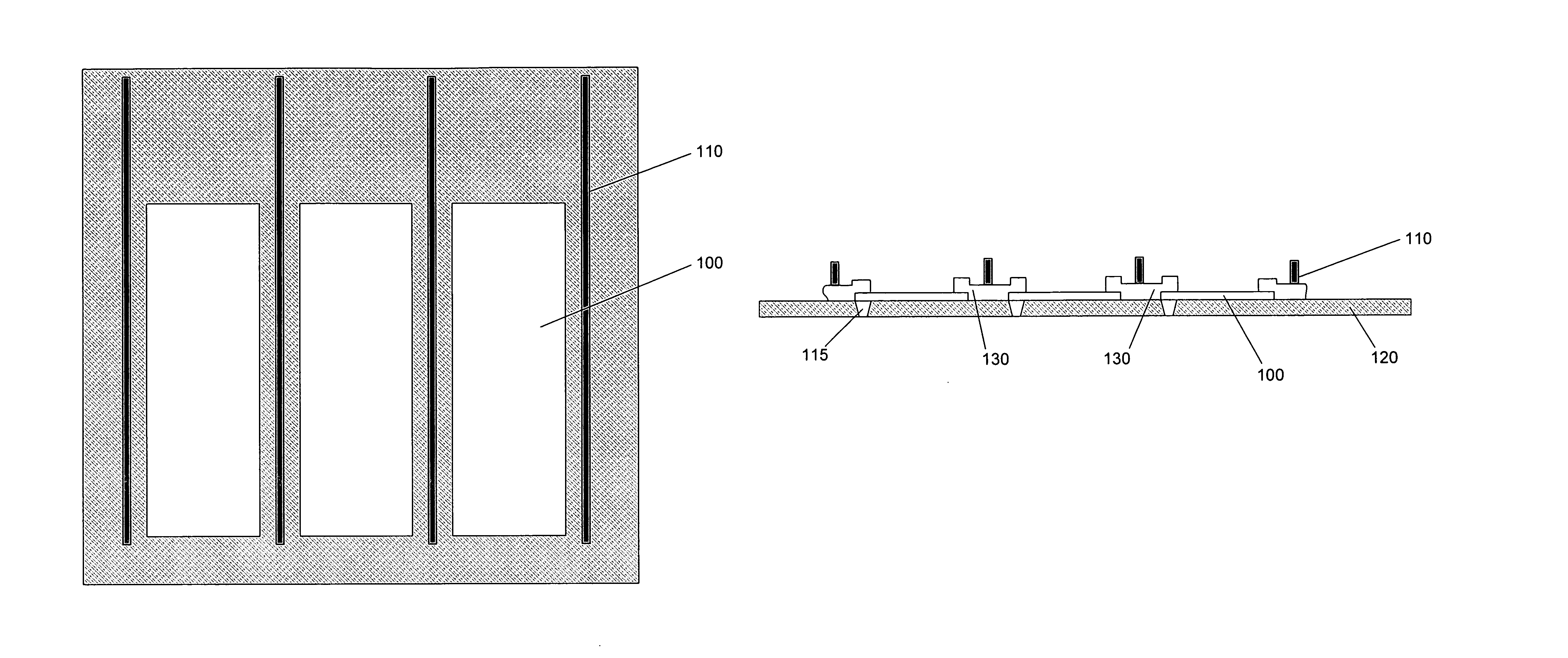
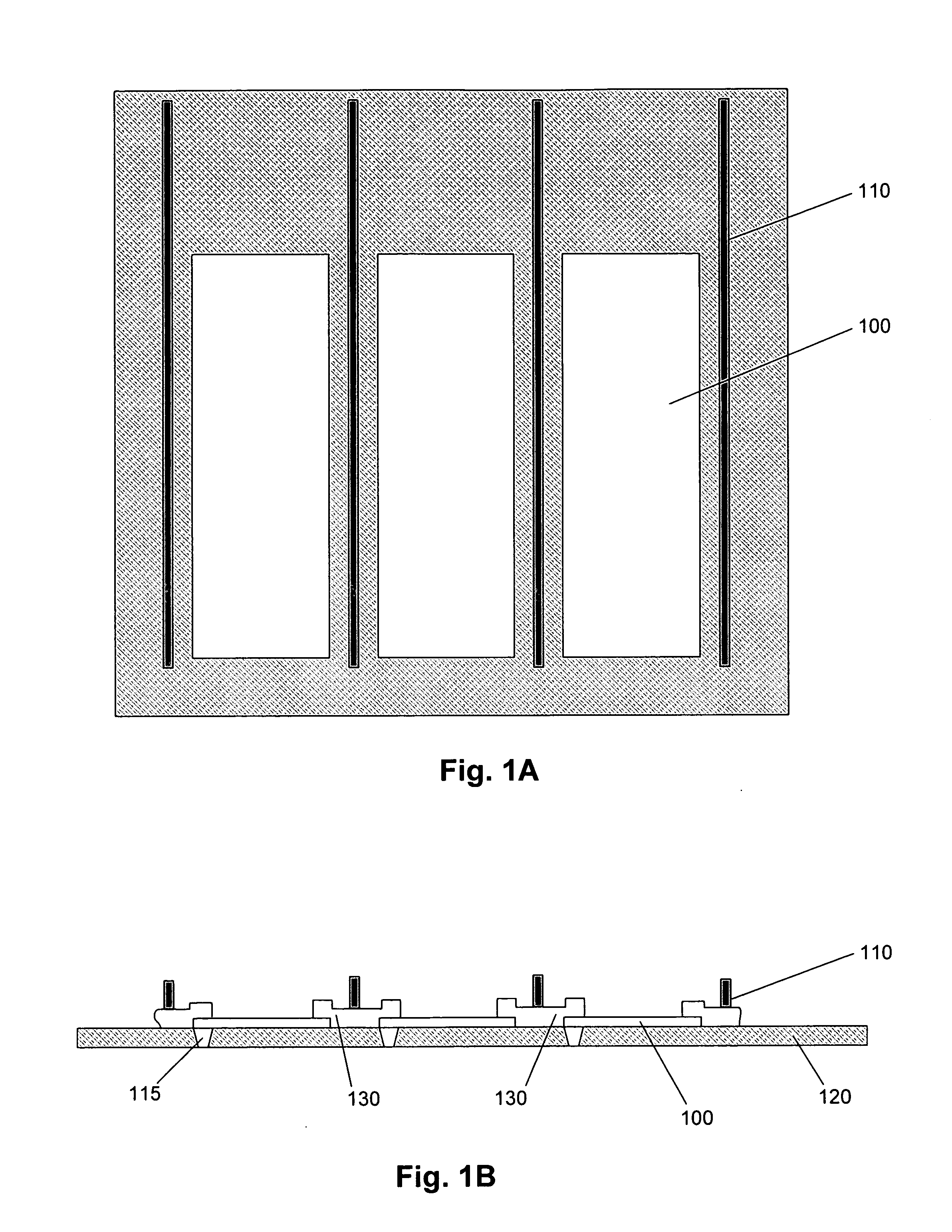
[0014]An organic device substrate is provided with a larger well size or wider channel width as compared to an emission area. This improves the effective aperture ratio, which improves the pixel intensity homogeneity.

[0015]In the fabrication of a display, such as an OLED display, the OLED layer stack is deposited on an electrode on the substrate. The electrode may be the anode and may comprise indium tin oxide (ITO). Desirably, the deposited films are of uniform thickness over the entire active area of the electrode. If the films are not uniform, then areas that are thicker will not emit light, and areas that are too thin may emit light in a less than optimum efficient way (power loss) and / or result in leakage current leaks through the device in a way that does not generate photons.

[0016]FIG. 1A is an overhead schematic diagram of an exemplary structure showing channel type wells in accordance with the present invention, and FIG. 1B is a cross-sectional view of the exemplary structu...


PUM


Abstract

In the fabrication of a display, such as an OLED display, the OLED layer stack is deposited on an electrode on the substrate. The electrode may be the anode and may comprise indium tin oxide (ITO). Desirably, the deposited films are of uniform thickness over the entire active area of the electrode. If the films are not uniform, then areas that are thicker will not emit light, and areas that are too thin may emit light in a less than optimum efficient way (power loss) and/or result in leakage current leaks through the device in a way that does not generate photons. An active-matrix organic light emitting diode comprises a substrate with a larger well size or wider channel width compared to the emission area. This improves the effective aperture ratio, which improves pixel intensity homogeneity.

Description

CROSS REFERENCE[0001]This application claims benefit to U.S. Provisional Application Ser. No. 60 / 640,812 filed Dec. 29, 2004, the disclosure of which is incorporated herein by reference in its entirety.FIELD[0002]This disclosure relates generally to organic electronic devices and more specifically to active-matrix organic light emitting diodes (OLEDs).BACKGROUND[0003]Organic electronic devices convert electrical energy into radiation, detect signals through electronic processes, convert radiation into electrical energy, or include one or more organic semiconductor layers. In the fabrication of a display, such as an OLED display, the OLED layer stack is deposited as films on an electrode on the substrate. If the films are not uniform, then areas that are thicker will not emit light, and areas that are too thin may emit light in a less than optimum efficient way and / or result in leakage current leaks through the device in a way that does not generate photons.[0004]Conventional active-...

Claims


Application Information

Patent Timeline
Patent Type & Authority Patents(United States)
IPC IPC(8): H05B33/14H01L21/20H05B33/00
CPCH01L27/3246H01L27/326H01L51/0005H01L51/5012H01L2251/558H10K59/121H10K59/122H10K71/135H10K50/11H10K2102/351
Inventor STAINER, MATTHEWPARKER, IAN D.INNOCENZO, JEFFREY G.YU, GANG
Owner LG CHEM LTD
Why Eureka
Try Eureka