LCD device including an insulator film having a contact hole for exposing a pixel electrode

a liquid crystal display and contact hole technology, applied in static indicating devices, instruments, non-linear optics, etc., can solve the problems of uneven surface, reduced contrast ratio of lcd devices, uneven surface, etc., to achieve small leakage light, increase the effective aperture ratio, and reduce the effect of pixel effective aperture ratio

Active Publication Date: 2012-02-21
NEC LCD TECH CORP
View PDF19 Cites 2 Cited by
  • Summary
  • Abstract
  • Description
  • Claims
  • Application Information

AI Technical Summary

Benefits of technology

[0015]In view of the above, it is an object of the present invention to provide a LCD device solving the above problem and having a smaller leakage light, a higher effective aperture ratio and a higher contrast ratio.

Problems solved by technology

Although the IPS-mode LCD device can realize a higher viewing angle characteristic, there is a problem that a coloring phenomenon occurs upon display of a bright state as viewed in a slanted direction.
The step difference formed on the surface of the alignment film by the presence and absence of the electrodes may incur an obstacle against a smooth rubbing treatment, to cause an uneven surface of the alignment film.
The uneven surface reduces the contrast ratio of the LCD device.
In addition, the uneven surface may incur a dead space between the pattern of the TFT substrate and the counter substrate, thereby reducing the effective aperture ratio of each pixel.
Furthermore, a deviation in the angle between the optical axis of the polarizing films and the extending direction of the electrodes causes an optical diffraction at the edge of the electrodes, deviates the direction of polarization to generate leakage light, and thus reduces the contrast ratio.

Method used


Image

  • LCD device including an insulator film having a contact hole for exposing a pixel electrode
  • LCD device including an insulator film having a contact hole for exposing a pixel electrode
  • LCD device including an insulator film having a contact hole for exposing a pixel electrode

Examples


first embodiment

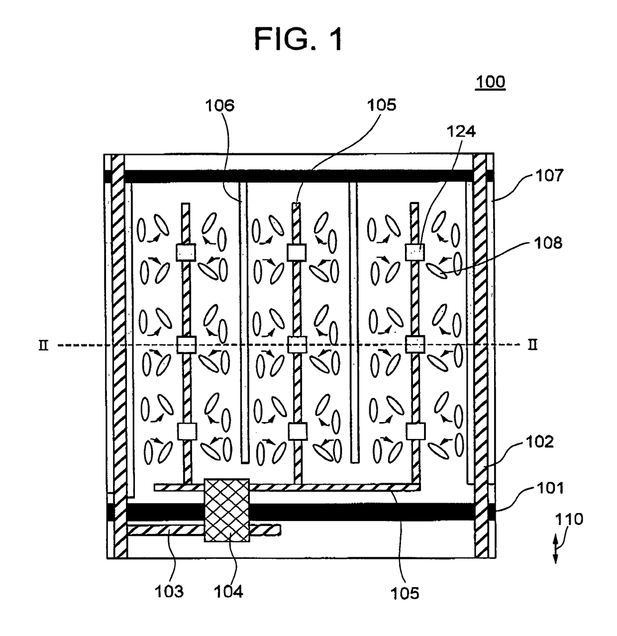
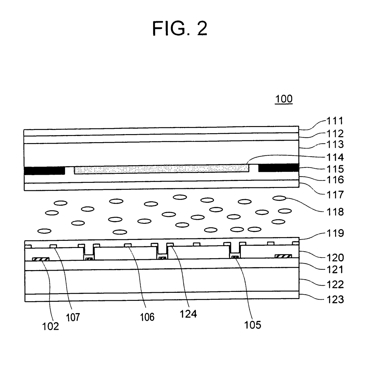
[0029]FIG. 1 shows the arrangement of electrodes in the pixel of a LCD device according to the present invention in a top plan view, and FIG. 2 shows a sectional view taken along line II-II in FIG. 1. The LCD device, generally designated at numeral 100, includes a first transparent substrate (glass substrate) 122 on which TFTs are formed, a second transparent substrate 113 opposing the first transparent substrate, and a LC layer 118 disposed between both the substrates 122 and 113. The first transparent substrate 122 includes thereon a plurality of gate electrodes (gate lines) 101 extending in a row direction, a plurality of data lines 102 extending in a column direction, and an array of pixels and an array of associated TFTs 104 disposed in the vicinity of the intersections of the gate lines and data lines. One of the pixels and an associated TFT are shown in FIG. 1. Each pixel includes a pixel electrode 105 and a common electrode 106.

[0030]On the first transparent substrate 122 ar...

fourth embodiment

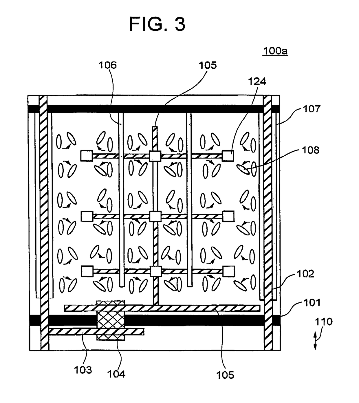
[0043]FIG. 5 shows the arrangement of electrodes in the pixel of a LCD device according to the present invention in a top plan view. The LCD device 100c of the present embodiment is such that control electrodes 124 are formed for both the pixel electrode 105 and common electrode 106. The control electrodes 124 are arranged in a staggered configuration, wherein the control electrodes 124 of the common electrode 106 are located on a line passing the center between adjacent control electrodes 124 of the pixel electrode 105 in the row direction. The function of the control electrodes 124 of the common electrode 106 is similar to that of the pixel electrode 105.

[0044]FIG. 6 shows the arrangement of electrodes in the pixel of a LCD according to a fifth embodiment of the present invention in a top plan view. The LCD device 100d of the present embodiment is such that the control electrodes 124 is of a square shape having a diagonal line parallel to the column or row direction of the LCD dev...


PUM

PropertyMeasurementUnit
areasaaaaaaaaaa
radial electric fieldaaaaaaaaaa
transparentaaaaaaaaaa

Abstract

A liquid crystal display (LCD) device includes first and second substrates, a liquid crystal (LC) layer sandwiched between the first substrate and the second substrate, the first substrate defining an array of pixel areas, each of the pixel areas including a pixel electrode and a common electrode, and an insulator film formed on the first substrate and on the pixel electrode, the insulator film including a contact hole and the pixel electrode being exposed through the contact hole such that a voltage supplied to the pixel electrode generates a radial electric field around the contact hole and between the pixel electrode and the common electrode.

Description

[0001]This application is based upon and claims the benefit of priority from Japanese patent application No. 2006-201392, the disclosure of which is incorporated herein in its entirety by reference.BACKGROUND OF THE INVENTION[0002](a) Field of the Invention[0003]The present invention relates to a lateral-electric-field-mode liquid crystal display (LCD) device and, more particularly, to a LCD device wherein liquid crystal (LC) molecules in a LC layer are rotated in a plane parallel to both the surface of the substrates sandwiching therebetween the LC layer.[0004](b) Description of the Related Art[0005]Active-matrix (AM) LCD devices are known in the art wherein active elements, such as thin-film-transistors (TFTs), are used as switching devices for controlling respective pixels. The AM LCD device has a high-definition image quality, and is widely used as a monitor of a desktop computer, etc. Typical operational modes of the LCD device include: a twisted-nematic (TN) mode in which the ...

Claims


Application Information

Patent Timeline
Patent Type & Authority Patents(United States)
IPC IPC(8): G02F1/1343G02F1/1333
CPCG02F1/134363G02F2001/134318G02F1/134318
Inventor MIZOGUCHI, CHIKAAKI
Owner NEC LCD TECH CORP
Why Eureka
Try Eureka