Liquid crystal display

a liquid crystal display and liquid crystal technology, applied in non-linear optics, instruments, optics, etc., can solve the problems of unstable directionality of liquid crystals, difficult to effectively control liquid crystals, poor lateral visibility, etc., to reduce the response time of liquid crystals, improve the light transmission of each pixel, and increase the effective aperture ratio of each pixel

Active Publication Date: 2009-08-06
SAMSUNG DISPLAY CO LTD
View PDF4 Cites 3 Cited by
  • Summary
  • Abstract
  • Description
  • Claims
  • Application Information

AI Technical Summary

Benefits of technology

[0009]Aspects of the present invention in accordance with various embodiments provide a liquid crystal display (LCD) with reduced response time of liquid crystals, increased effective aperture ratio of each pixel, and thus improved light transmission of each pixel.

Problems solved by technology

However, since their lateral visibility is poor compared to front visibility, various methods of arranging liquid crystals and various driving methods are being developed to overcome this drawback.
In this case, however, it is difficult to effectively control liquid crystals since the gap between electrodes increases.
Thus, the directionality of the liquid crystals is unstable.
Such unstable directionality of liquid crystals creates texture, reduces luminance, and increases response time.

Method used


Image

  • Liquid crystal display
  • Liquid crystal display
  • Liquid crystal display

Examples


first embodiment

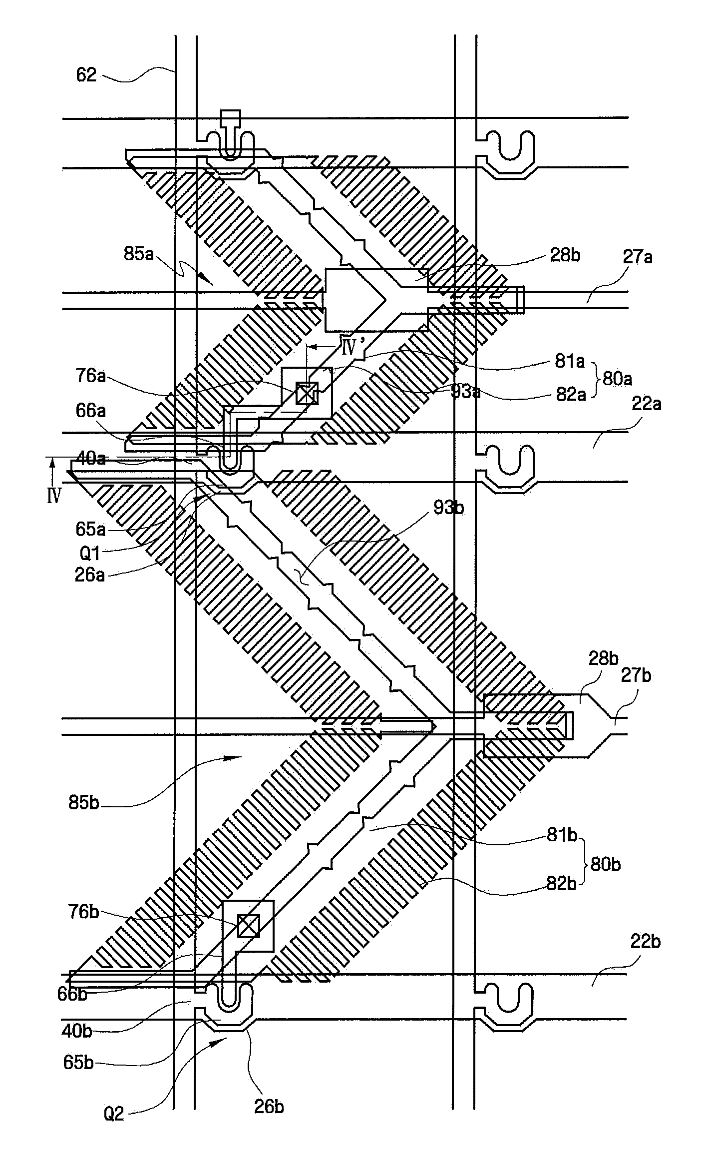
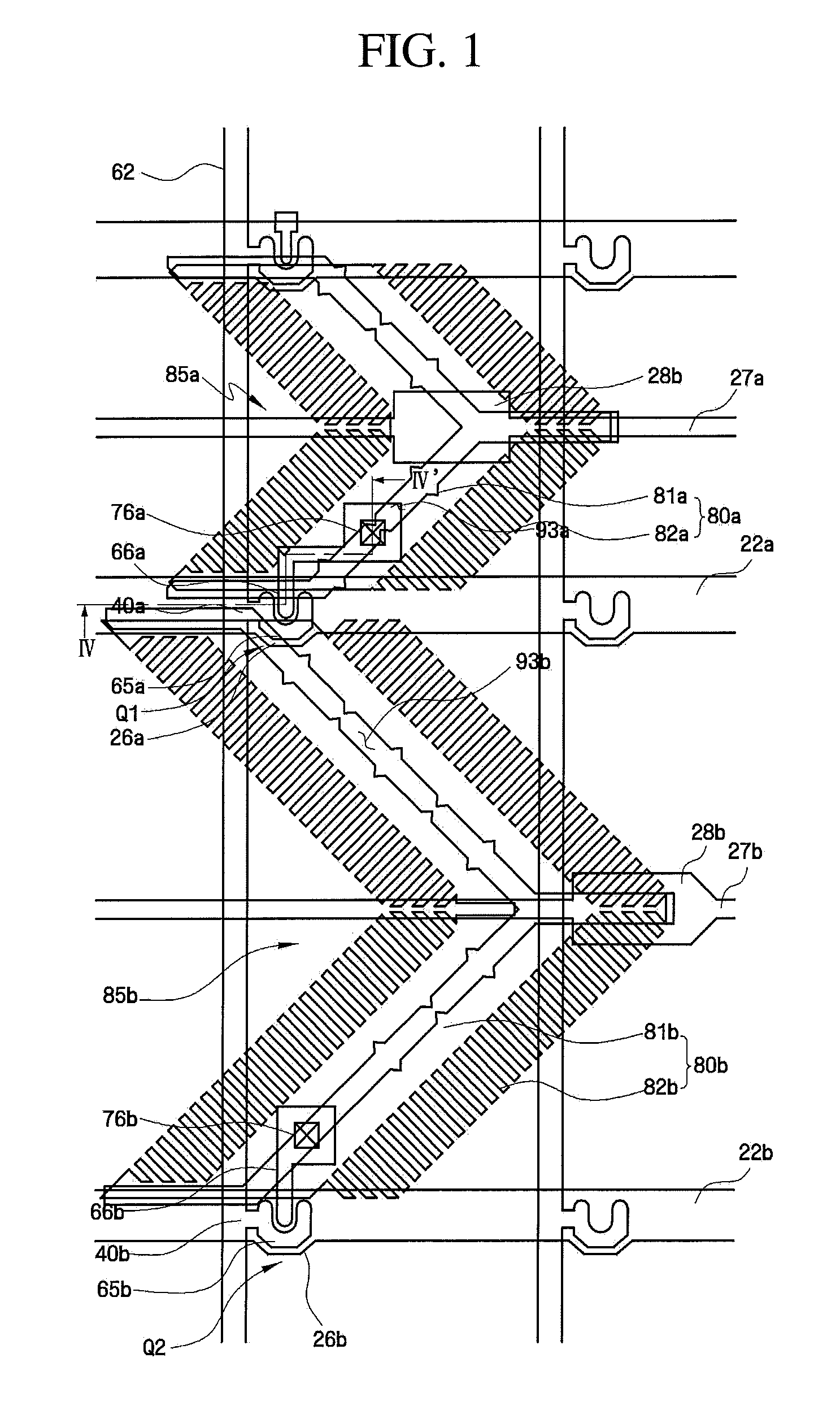
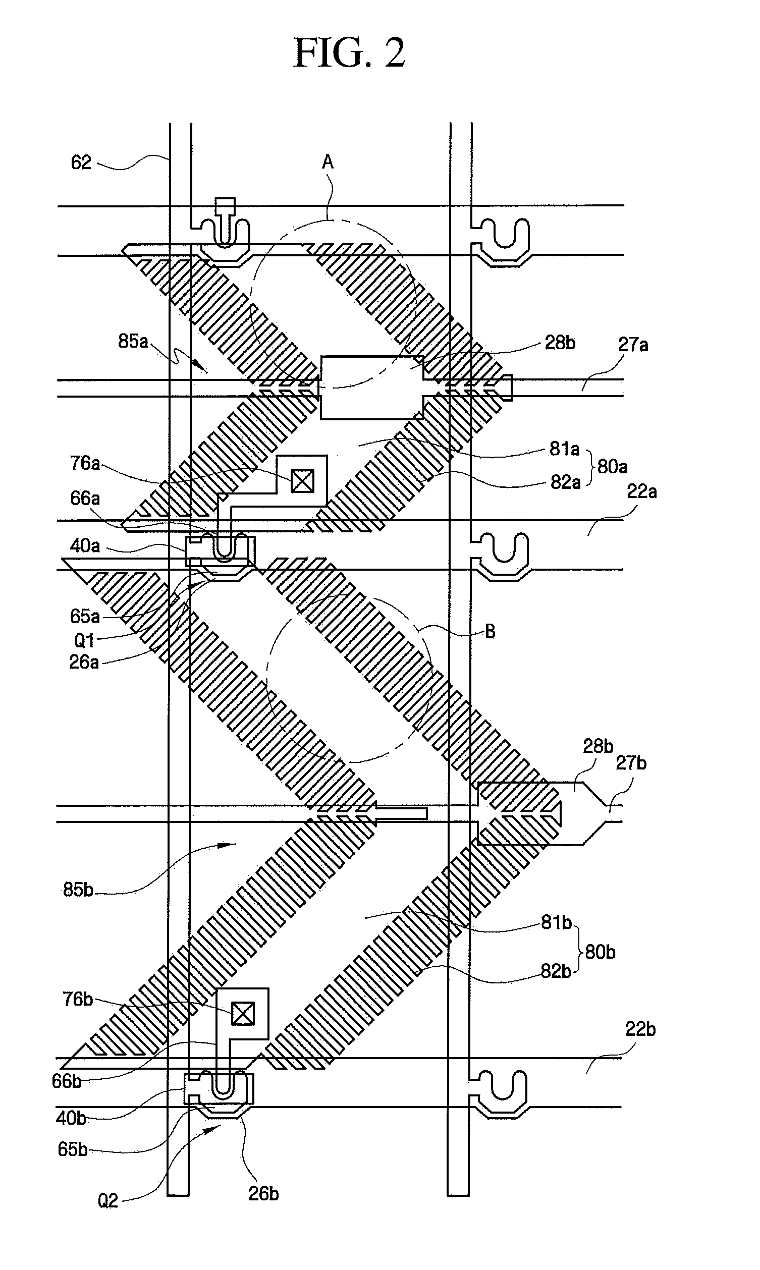
[0028]Hereinafter, a liquid crystal display (LCD) according to one embodiment will be described in detail with reference to FIGS. 1 through 6B. FIG. 1 is an arrangement plan of the LCD according to the present invention. FIG. 2 is an arrangement plan of a thin-film transistor (TFT) display plate 100 of the LCD shown in FIG. 1. FIG. 3 is an arrangement plan of a common electrode display plate 200 of the LCD shown in FIG. 1. FIG. 4 is a cross-sectional view of the LCD taken along a line IV-IV′ of FIG. 1.

[0029]Referring to FIGS. 1 through 4, the LCD according to the first embodiment includes a TFT display plate 100, a common electrode display plate 200 facing the TFT display plate 100, and a liquid crystal layer 300 interposed between the TFT display plate 100 and the common electrode display plate 200.

[0030]First and second gate lines 22a and 22b are formed on a first insulating substrate 10 which is made of transparent glass. The first and second gate lines 22a and 22b generally exte...

second embodiment

[0069]Referring to FIGS. 7 through 9, the LCD includes a first subpixel electrode 80a_1, which does not have fine patterns; a second subpixel electrode 80b_1, which has fine patterns; and a common electrode 191 which has fine patterns at a location corresponding to the first subpixel electrode 80a_1.

[0070]The TFT display plate includes first and second gate lines 22a_1 and 22b_1 formed on a first insulating substrate 10. The first and second gate lines 22a_1 and 22b_1 extend horizontally and parallel to each other. The TFT display plate also includes a data line 62_1 which crosses the first and second gate lines 22a_1 and 22b_1. The first and second gate lines 22a_1 and 22b_1 have first and second gate electrodes 26a_1 and 26b_1, respectively.

[0071]First and second subpixel electrodes 80a_1 and 80b_1 may be bent in a zigzag manner and may be separated from each other by a slit 86_1 which is a domain formation portion. However, the domain formation portion may not be limited to the ...

third embodiment

[0075]Referring to FIG. 10, the LCD includes a first subpixel electrode 80a_2 having a plurality of first fine protruding patterns 82a_2 separated from each other by a first gap 83a_2, and a second subpixel electrode 80b_2 having a plurality of second fine protruding patterns 82b_1 separated from each other by a second gap 83b_2. A length of each of the first fine protruding patterns 82a_1 may be greater than that of each of the second fine protruding patterns 82b_1. In addition, the sum of a width of each of the first fine protruding patterns 82a_1 and a width of the first gap 83a_1 may be greater than the sum of a width of each of the second fine protruding patterns 82b_2 and a width of the second gap 83b_2.

[0076]The first and second subpixel electrodes 80a_2 and 80b_2 may be bent in a zigzag manner and may be separated from each other by a slit 86_2 which is a domain formation portion.

[0077]The first subpixel electrode 80a_2 includes a first flat portion 81a_2 in the middle ther...


PUM

PropertyMeasurementUnit
widthaaaaaaaaaa
voltageaaaaaaaaaa
areaaaaaaaaaaa

Abstract

Provided is a liquid crystal display (LCD), the LCD includes: an insulating substrate; a first gate line and a second gate line which are formed on the insulating substrate and extend parallel to each other; a data line formed on the insulating substrate, insulated from the first and second gate lines, and crosses the first and second gate lines; a first subpixel electrode connected to the first gate line and the data line by a first switching device and includes a plurality of first fine protruding patterns at an edge thereof; and a second subpixel electrode connected to the second gate line and the data line by a second switching device and includes a plurality of second fine protruding patterns at an edge thereof, wherein the first fine protruding patterns are separated from each other by a first gap, and the second fine protruding patterns are separated from each other by a second gap, wherein the sum of a width of the first gap and a width of each of the first fine protruding patterns is greater than the sum of a width of the second gap and a width of each of the second protruding patterns.

Description

[0001]This application claims priority and benefit under 35 U.S.C. §119 to Korean Patent Application No. 10-2008-0009738, filed on Jan. 30, 2008 in the Korean Intellectual Property Office, the disclosure of which is incorporated herein by reference in its entirety.BACKGROUND[0002]1. Technical Field[0003]Embodiment of the present invention relate to a liquid crystal display (LCD), and more particularly, to an LCD with reduced response time of liquid crystals, increased effective aperture ratio of each pixel, and thus improved light transmission of each pixel.[0004]2. Description of the Related Art[0005]Liquid crystal displays (LCDs) are one of the most widely used flat panel displays (FPDs). An LCD includes two substrates, on which electrodes are formed, and a liquid crystal layer interposed between the two substrates. The LCD rearranges liquid molecules of the liquid crystal layer by applying voltage to the electrodes and thus controls the amount of light transmitted. In this way, t...

Claims


Application Information

Patent Timeline
Patent Type & Authority Applications(United States)
IPC IPC(8): G02F1/1343
CPCG02F1/134336G02F1/134363G02F2001/134345G02F1/13624G02F1/134345G02F1/1343
Inventor KIM, DONG-GYUJUN, SAHNG-IKBAEK, SEUNG-SOOPARK, KEE-BUM
Owner SAMSUNG DISPLAY CO LTD
Why Eureka
Try Eureka