Solid-state image pickup device

a solid-state image and pickup device technology, applied in the direction of television systems, picture signal generators, radioation control devices, etc., can solve the problems of mixing colors, difficult to obtain sufficient sensitivity, and difficulty in obtaining sufficient utilization efficiency of incident ligh

Inactive Publication Date: 2013-12-10
KK TOSHIBA
View PDF23 Cites 4 Cited by
  • Summary
  • Abstract
  • Description
  • Claims
  • Application Information

AI Technical Summary

Benefits of technology

[0005]To solve such problems, there has been proposed a back side radiation type image sensor which is such that a photodiode is irradiated with light from the back surface side (the side opposite to an interconnect layer) and high sensitivity is obtained by increasing the effective aperture ratio without the influence of the presence of the interconnect layer and the like.

Problems solved by technology

However, because the aperture size of a photodiode with respect to a surface of incidence of light is limited by the presence of the interconnect layers, with the pitch of pixels miniaturized, it has been difficult to obtain sufficient utilization efficiencies of incident light.
However, with the trends toward high integration and scaledown of semiconductor devices growing stronger, it has become difficult to obtain sufficient sensitivity even by using microlenses.
For this reason, light that has not been absorbed by a pixel for red color reaches a green pixel and a blue pixel, which are adjacent to the red pixel, thereby posing the problem of what is called mixing of colors in which a wrong color signal is given.
Also, in the back side radiation type, light (that has not been absorbed in Si) reflected from the interconnect layer positioned below the photodiode penetrates into an adjacent pixel and this may cause mixing of colors.
As described above, conventional back side radiation type image sensors as described above had the problem that mixing of colors is apt to occur.

Method used


Image

  • Solid-state image pickup device
  • Solid-state image pickup device
  • Solid-state image pickup device

Examples


Embodiment Construction

[0037]A solid-state image pickup device in an embodiment of the present invention will be described below on the basis of the drawings.

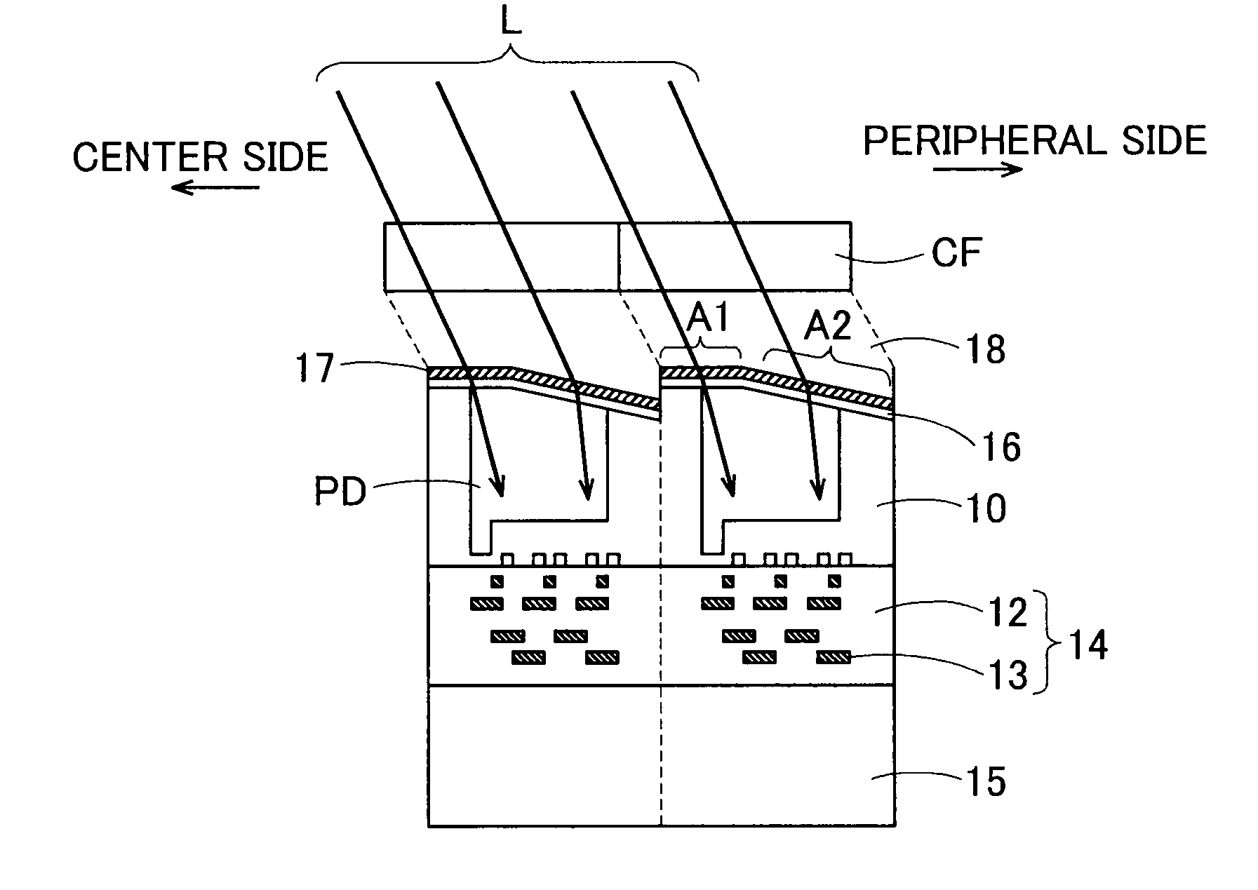
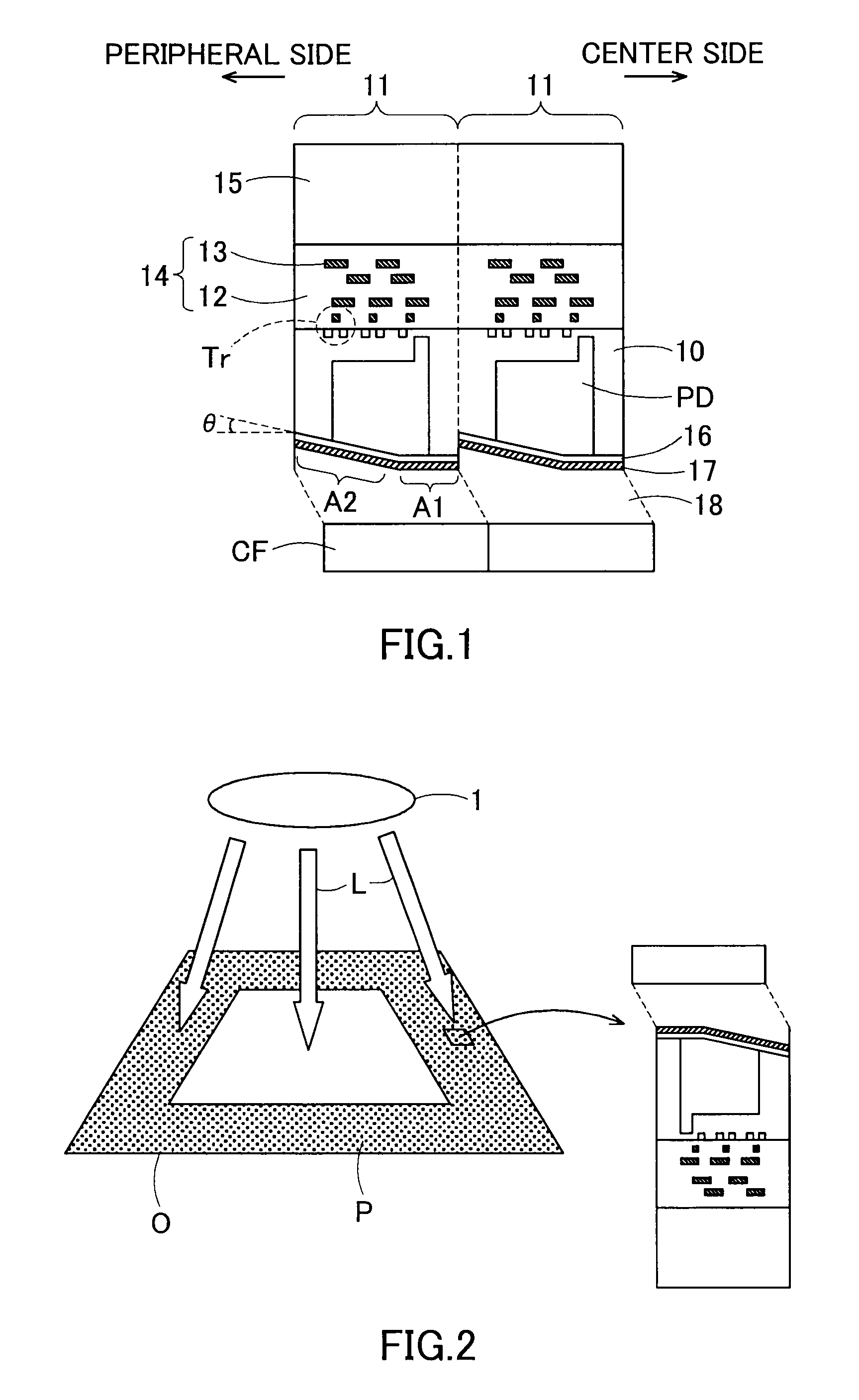
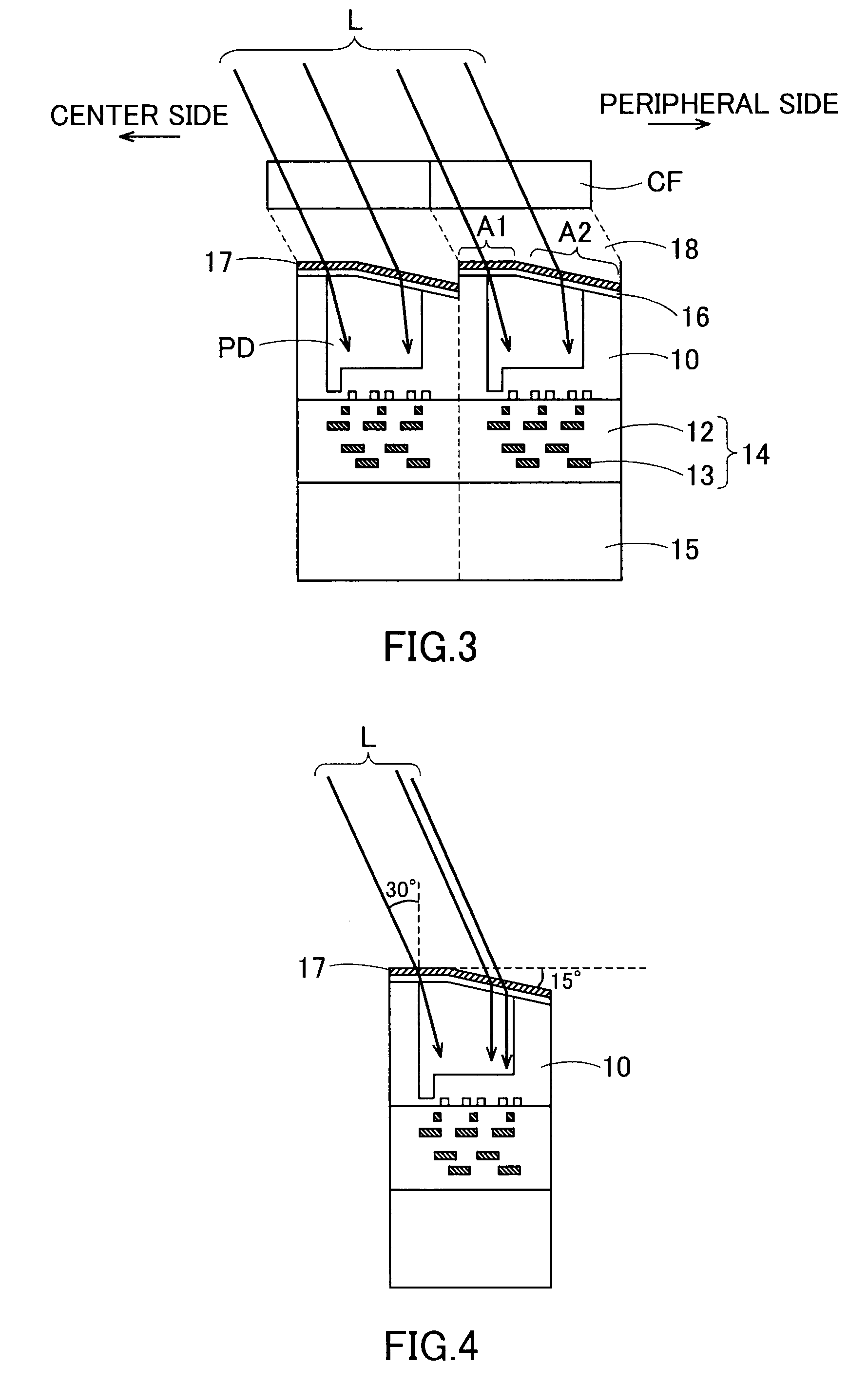
[0038]FIG. 1 shows a longitudinal sectional view of a solid-state image pickup device related to an embodiment of the present invention. The solid-state image pickup device related to this embodiment is a back side radiation type CMOS solid-state image pickup device.

[0039]In this solid-state image pickup device, upon a substrate 10, which is, for example, a silicon semiconductor substrate, there are formed in a matrix manner a plurality of unit pixels 11, each having a photodiode PD and a plurality of MOS transistors Tr, which become means of performing the reading-out, amplification, resetting and the like of a signal charge of this photodiode PD.

[0040]As shown in FIG. 2, a description will be given here of pixels in a peripheral part P of a pixel region O in which the incident angle of light L from an image optics system 1 is large.

[0041]Upon the f...


PUM


Abstract

A solid-state image pickup device has a photoelectric conversion element that converts light incident from a first surface of a substrate into a signal charge and accumulates the signal charge, a transistor that is formed on a second surface side opposite to the first surface of the substrate and reads out the signal charge accumulated by the photoelectric conversion element, a supporting substrate stuck to the second surface of the substrate, and an antireflection coating formed on the first surface of the substrate, wherein the first surface of the substrate includes a curved surface or an inclined surface forming a prescribed angle to the second surface.

Description

CROSS REFERENCE TO RELATED APPLICATION[0001]This application is based upon and claims benefit of priority from the Japanese Patent Application No. 2008-78228, filed on Mar. 25, 2008, the entire contents of which are incorporated herein by reference.BACKGROUND OF THE INVENTION[0002]The present invention relates to a solid-state image pickup device.[0003]In conventional CMOS image sensors, a plurality of photoelectric conversion parts (photodiodes) that become pixels are formed in a matrix manner in a front surface portion of a semiconductor substrate, and light is radiated (caused to become incident) to the photodiodes by being caused to pass through the gaps of interconnect layers, whereby the light is detected. However, because the aperture size of a photodiode with respect to a surface of incidence of light is limited by the presence of the interconnect layers, with the pitch of pixels miniaturized, it has been difficult to obtain sufficient utilization efficiencies of incident li...

Claims


Application Information

Patent Timeline
Patent Type & Authority Patents(United States)
IPC IPC(8): H01L27/146H01L27/14H04N5/335H04N5/357H04N5/369H04N5/374H04N9/07
CPCH01L27/1464H01L27/1462H01L27/14605
Inventor UENO, RISAKOFUNAKI, HIDEYUKIIIDA, YOSHINORIHONDA, HIROTO
Owner KK TOSHIBA
Why Eureka
Try Eureka