Inorganic light emitting display

Active Publication Date: 2008-09-18
SAMSUNG DISPLAY CO LTD
View PDF16 Cites 0 Cited by
  • Summary
  • Abstract
  • Description
  • Claims
  • Application Information

AI Technical Summary

Benefits of technology

[0009]Aspects of the present invention provide an inorganic light

Problems solved by technology

Accordingly, since a large number of electrons should be accelerated at a high energy to achieve a high efficiency, the inorganic light emitting display has the disadvantage of requiring a high driving voltage.
Also, since pla

Method used


Image

  • Inorganic light emitting display
  • Inorganic light emitting display
  • Inorganic light emitting display

Examples


Example

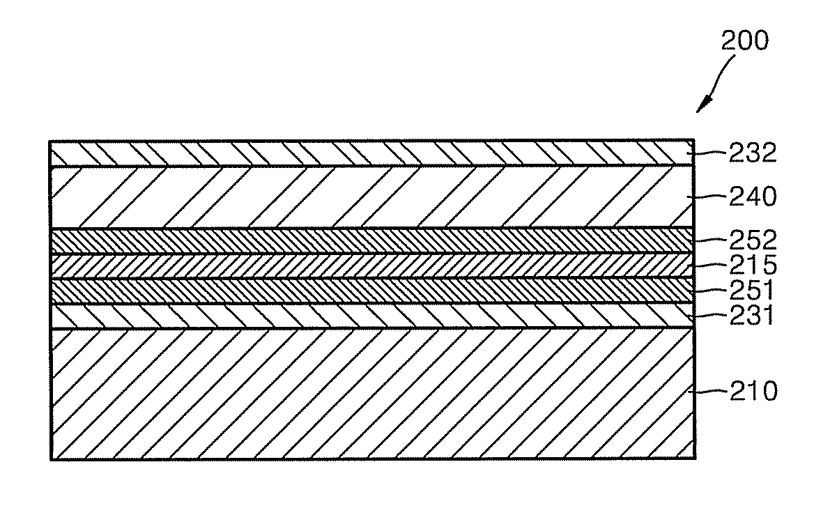
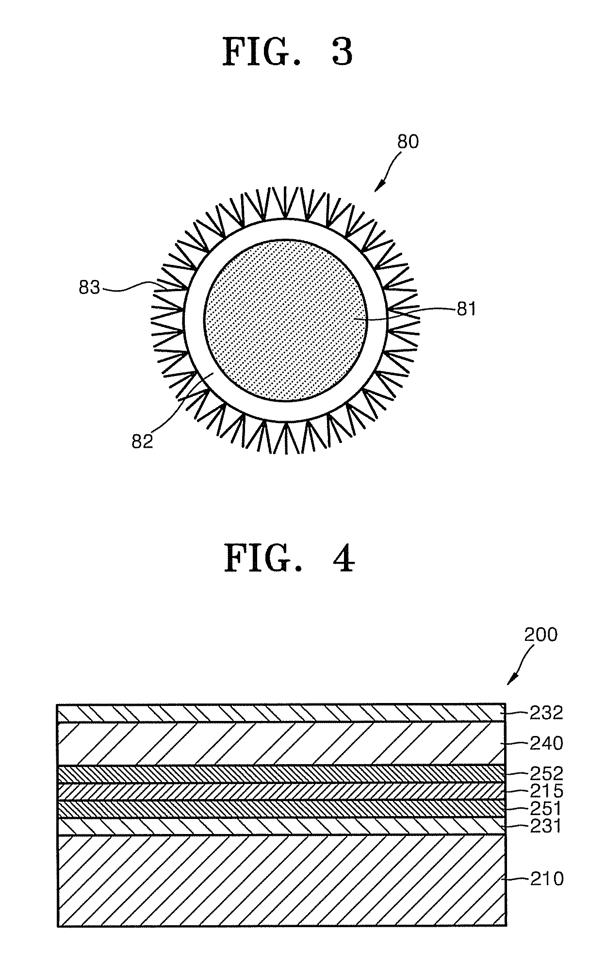
[0020]Reference will now be made in detail, to exemplary embodiments of the present invention, examples of which are illustrated in the accompanying drawings, wherein like reference numerals refer to the like elements throughout. The exemplary embodiments are described below, in order to explain the aspects of present invention, by referring to the figures.

[0021]It will be understood that when a layer or element is referred to as being disposed “on” another layer or substrate, it can be directly on the other layer or substrate, or intervening layers may also be present. Further, it will be understood that when a layer is referred to as being disposed “under” another layer, it can be directly under, and one or more intervening layers may also be present. In addition, it will also be understood that when a layer is referred to as being disposed “between” two layers, it can be the only layer between the two layers, or one or more intervening layers may also be present.

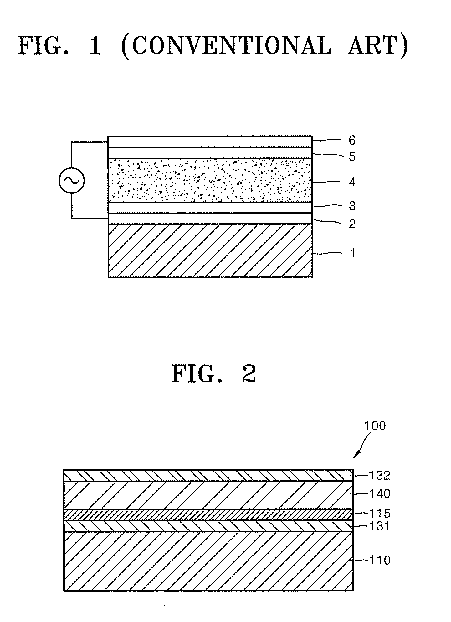
[0022]FIG. 2 is a...


PUM


Abstract

An inorganic light emitting display including: a first electrode; a second electrode facing the first electrode; a light emitting layer disposed between the first electrode and the second electrode; and an field emission layer disposed between the light emitting layer and the second electrode.

Description

CROSS-REFERENCE TO RELATED APPLICATION[0001]This application claims the benefit of Korean Application No. 2007-24695, filed Mar. 13, 2007, in the Korean Intellectual Property Office, the disclosure of which is incorporated herein by reference.BACKGROUND OF THE INVENTION[0002]1. Field of the Invention[0003]Aspects of the present invention relate to an inorganic light emitting display.[0004]2. Description of the Related Art[0005]Recently, research has been conducted on inorganic light emitting displays in a wide variety of areas. Conventional inorganic light emitting displays are disclosed in U.S. Pat. Nos. 5,543,237 and 5,648,181. The disclosed inorganic light emitting display is configured as shown in FIG. 1.[0006]An indium tin oxide (ITO) electrode 2 is formed on a substrate 1, and a first dielectric layer 3 is formed on the ITO electrode 2. An inorganic light emitting layer 4 is formed on the first dielectric layer 3, and a second dielectric layer 5 and a rear electrode 6 are sequ...

Claims


Application Information

Patent Timeline
IPC IPC(8): H01J1/62
CPCH01J29/28H01J2329/0444H01J2329/007H01J31/127H05B33/14H05B33/20
Inventor KIM, YOON-JINKIM, JAE-MYUNGMOON, HEE-SUNGNAM, MUN-HOPARK, HYOUNG-BINSON, SEUNG-HYUN
Owner SAMSUNG DISPLAY CO LTD
Why Eureka
Try Eureka