Method for Manufacturing Light-Emitting Device

a technology of light-emitting devices and manufacturing methods, which is applied in the direction of semiconductor devices, basic electric elements, electrical apparatus, etc., can solve the problems of long time (or takt time) taken for the manufacture of full-color organic el panels, and achieve the effect of low power consumption of full-color display devices

Inactive Publication Date: 2008-09-25
SEMICON ENERGY LAB CO LTD
View PDF16 Cites 19 Cited by
  • Summary
  • Abstract
  • Description
  • Claims
  • Application Information

AI Technical Summary

Benefits of technology

[0015]It is an object of the present invention to provide a technique for forming a film with high thickness uniformity, using an apparatus having a relatively simple structure. In addition, it is an object of the present invention to provide a technique for greatly shortening the period of time taken to manufacture a full-color organic EL panel. It is an object of the present invention to reduce the loss of takt time or manufacturing cost with the use of these techniques.

Problems solved by technology

Thus, the total period of time (or takt time) taken for manufacture of a full-color organic EL panel has been long.

Method used


Image

  • Method for Manufacturing Light-Emitting Device
  • Method for Manufacturing Light-Emitting Device
  • Method for Manufacturing Light-Emitting Device

Examples


embodiment mode 1

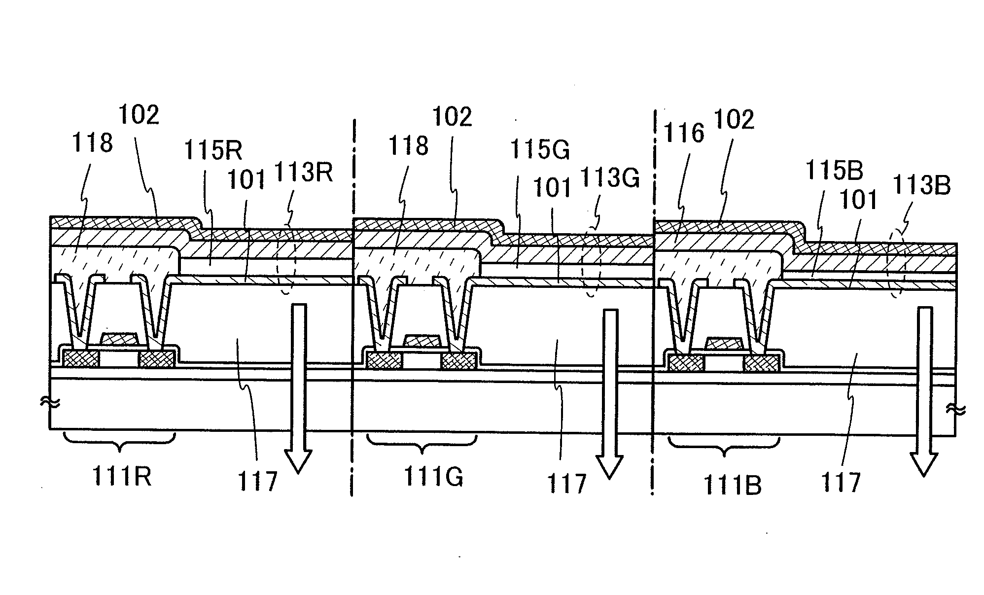
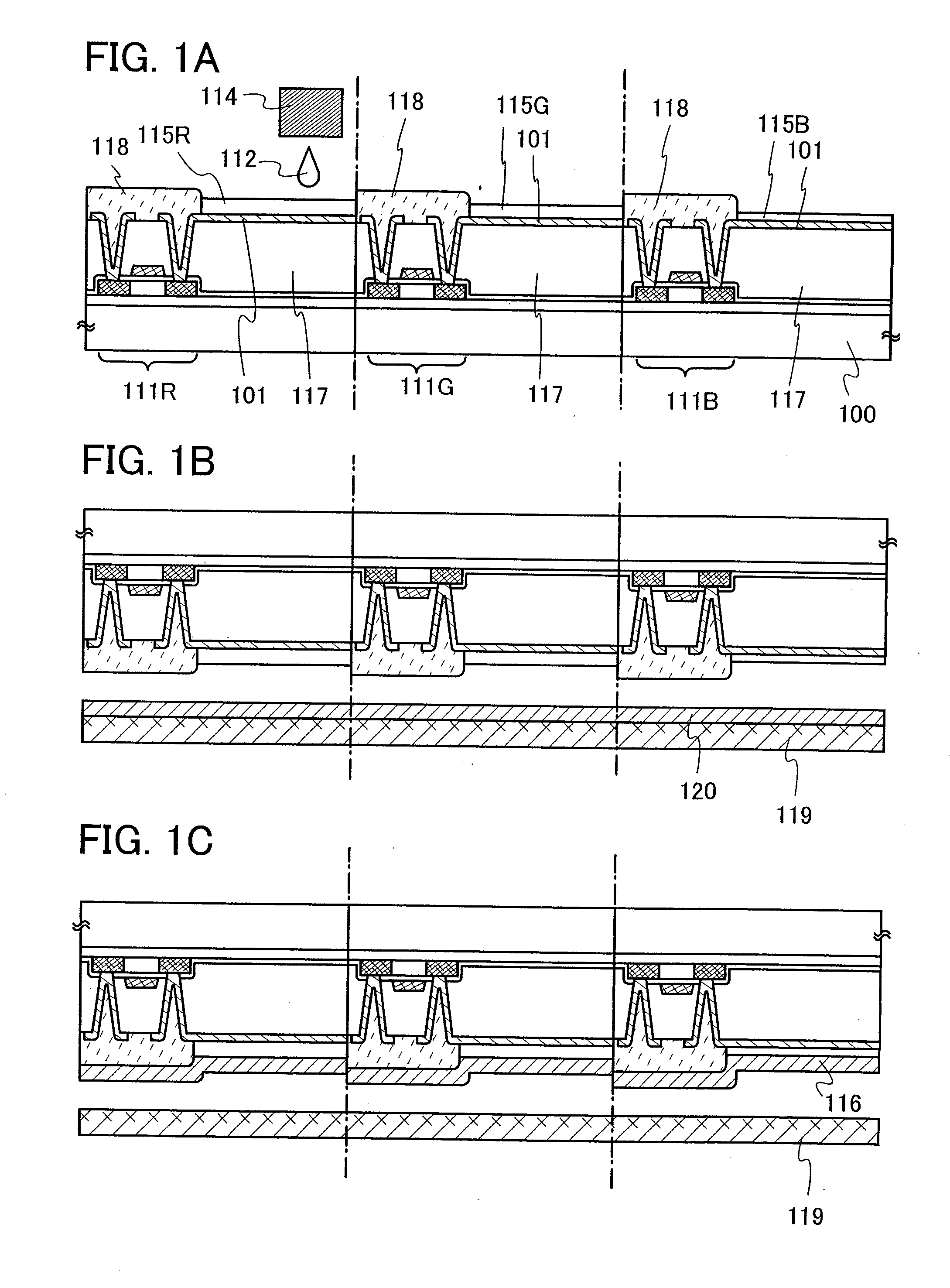
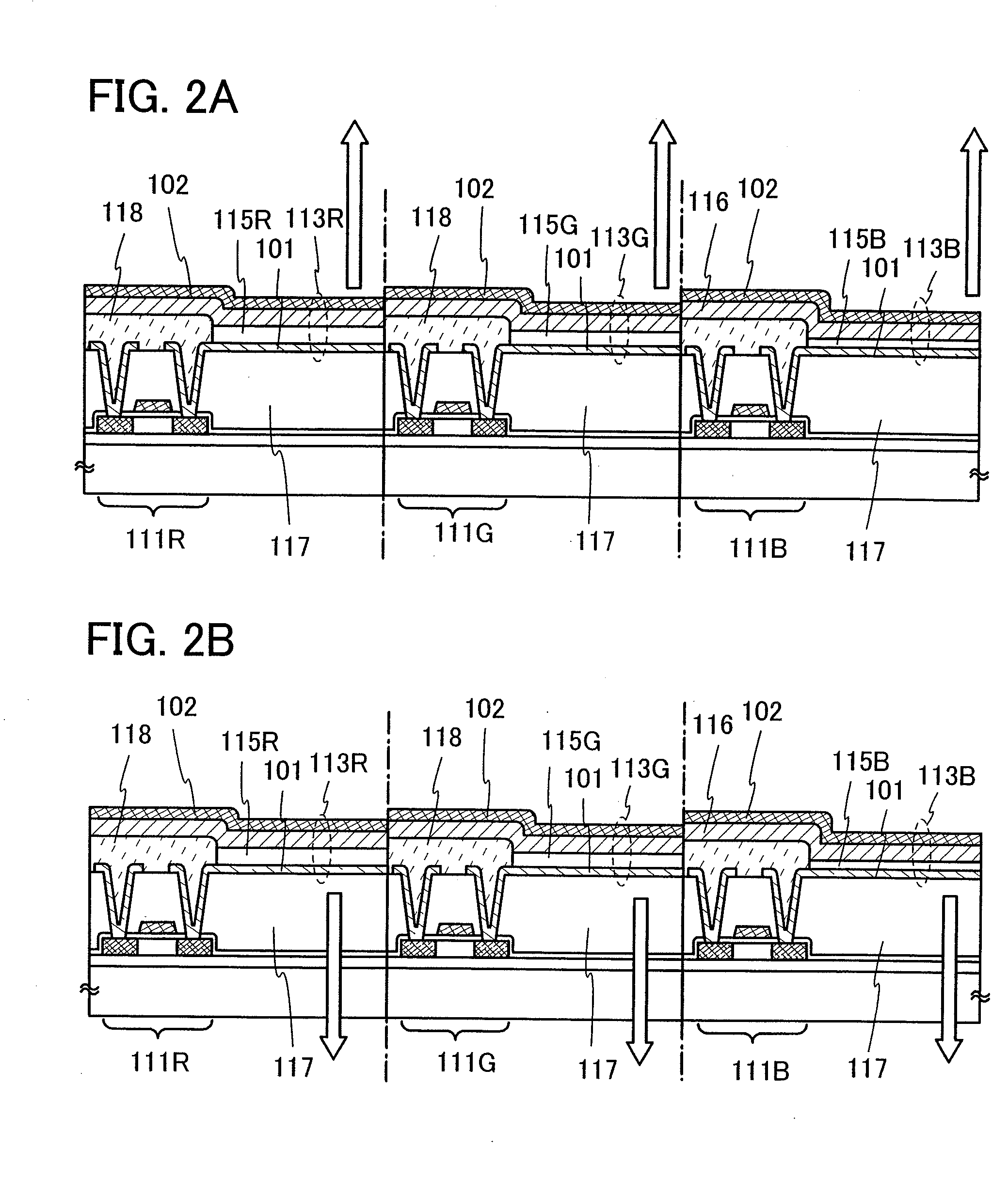
[0063]First, a plurality of TFTs is manufactured over a substrate having an insulating surface 100. The TFTs are transistors for controlling current supply to respective-color-light-emitting elements. In each of the TFTs, a semiconductor film, a gate insulating film covering the semiconductor film, a gate electrode, and an interlayer insulating film over the gate electrode are provided. TFTs 111R, 111G, and 111B are covered with an interlayer insulating film 117, and a bank 118 having an opening is formed over the interlayer insulating film 117 as shown in FIG. 1A. A first electrode 101 is partially exposed in the opening of the bank 118.

[0064]The interlayer insulating film 117 can be formed of an organic resin material, an inorganic insulating material, or an insulator including a Si—O—Si bond which is formed from a siloxane-based material (hereinafter referred to as a siloxane insulator). Siloxane insulator contains hydrogen as a substituent and may contain at least one kind of fl...

embodiment mode 2

[0084]In this embodiment mode, one example of a film-formation apparatus having a plasma generator for cleaning is shown in FIG. 3.

[0085]FIG. 3 is a cross-sectional view showing one example of a film-formation apparatus having a cleaning function. A film-formation chamber 501 is coupled to a vacuum exhaust process chamber, which is preferably evacuated by vacuum exhaust so as not to mix moisture or the like. Further, the film-formation chamber 501 is coupled to a reactive gas introduction system for introducing a gas for cleaning. Further, the film-formation chamber 501 is coupled to an inert gas introduction system for introducing an inert gas so that inside the film-formation chamber is made in the atmospheric pressure state.

[0086]Further, as a material for an inner wall of the film-formation chamber 501, aluminum, stainless steel (SUS: Steel special Use Stainless), or the like which has been electropolished to have a mirror surface is used because the degree of adsorption of an i...

embodiment 1

[0121]Size of a manufacturing apparatus can be reduced by the method for manufacturing a full-color display device of the present invention. In this embodiment, one example of a manufacturing apparatus for manufacturing a full-color display device is described using FIGS. 6, 7, and 8.

[0122]FIG. 6 is a top-plane view of a multi-chamber manufacturing apparatus, and FIG. 7 corresponds to a cross-sectional view taken along a dashed line A-B thereof.

[0123]First, an arrangement in the manufacturing apparatus is described using FIG. 6. A first load chamber 701 in which a first substrate (also called a plate) is set is coupled to a first film-formation chamber 702. The first film-formation chamber 702 is coupled to a first stock chamber 705 via a first gate valve 703, and to a second stock chamber 706 via a second gate valve 704. Further, the first stock chamber 705 is coupled to a carrier chamber 709 via a third gate valve 707. Further, the second stock chamber 706 is coupled to the carrie...


PUM

PropertyMeasurementUnit
distanceaaaaaaaaaa
transparentaaaaaaaaaa
roughnessaaaaaaaaaa

Abstract

A full-color light-emitting device is achieved with plural kinds of light-emitting elements in each of which a stacked layer of a first material layer formed selectively with a droplet discharge apparatus and a second material layer formed by vapor-deposition method using the conductive-surface plate on which a layer containing an organic compound is formed is provided between a pair of electrodes. The first material layer is a layer in which an organic compound and a metal oxide which is an inorganic compound are mixed. By adjusting the thickness of the first material layer of each light-emitting element, which is different depending on an emission color, a blue light emission component, a green light emission component, or a red light emission component among a plurality of components for white light emission can be selectively emphasized and taken out by light interference phenomenon.

Description

BACKGROUND OF THE INVENTION[0001]1. Field of the Invention[0002]The present invention relates to a light-emitting device using a light-emitting element which can provide fluorescence or phosphorescence when an electric field is applied to the element in which a film containing an organic compound (hereinafter referred to as an ‘organic compound layer’) is provided between a pair of electrodes, and a manufacturing method thereof. Note that the light-emitting device refers to an image display device, a light emission device, or a light source (including a lighting device). Further, the present invention relates to a manufacturing apparatus of a light-emitting device and a cleaning method of the manufacturing apparatus.[0003]2. Description of the Related Art[0004]In recent years, a light-emitting device having an EL element as a self-luminous light-emitting element has been actively developed. This light-emitting device is also called an organic EL display or an organic light-emitting ...

Claims


Application Information

Patent Timeline
Patent Type & Authority Applications(United States)
IPC IPC(8): H01L21/00
CPCH01L33/08H01L51/5048H01L27/3281H01L51/5265H01L51/5036H01L2924/0002H01L27/3244H01L2924/00H10K59/12H10K59/17H10K50/125H10K50/14H10K50/852
Inventor HIRAKATA, YOSHIHARUSATO, YOSUKEYOKOYAMA, KOHEIKUWABARA, HIDEAKIYAMAZAKI, SHUNPEI
Owner SEMICON ENERGY LAB CO LTD
Why Eureka
Try Eureka