Illuminating Device

a technology of illumination device and heat radiation property, which is applied in the direction of solid-state devices, semiconductor devices, lighting and heating apparatus, etc., can solve the problems of reducing unable to obtain predetermined reflection efficiency, and difficulty in forming metal films, so as to improve the heat radiation property, reduce the temperature difference and improve the heat conductance between the substrate and the reflector

Inactive Publication Date: 2008-10-02
TOSHIBA LIGHTING & TECH CORP
View PDF5 Cites 38 Cited by
  • Summary
  • Abstract
  • Description
  • Claims
  • Application Information

AI Technical Summary

Benefits of technology

[0023]With the illuminating device having the circuit pattern formed on the substrate and the reflector also formed on the substrate, the heat conductance between the substrate and the reflector is improved, the temperature difference between the substrate and the reflector can be reduced, the heat radiation property can be improved, the peeling of the substrate and the reflector can be suppressed to enable the optical characteristics to be maintained, and moreover, because the reflector-side fitting portion, formed at the periphery of the housing portion of the reflector that houses the light emitting element, can be used, for example, to mount a lens, the light emitting element, the reflector, and the lens can be positioned accurately to enable the optical characteristics to be stabilized, and the lens can be fixed reliably onto the reflector.
[0024]With the lens-side fitting portion of the lens fitted and welded onto the reflector-side fitting portion of the reflector, the light emitting element, the reflector, and the lens can be positioned accurately to enable the optical characteristics to be stabilized and the lens can be fixed reliably onto the reflector.
[0025]With the reflector supported on the substrate by the supporting portions that are formed by making the resin flow into the anchoring-portion-provided penetrating holes ...

Problems solved by technology

Also, although a metal film is formed on the inner surface of each housing portion of the substrate to improve the reflection efficiency, it is difficult to form the metal film uniformly on the inner surface of the housing portion, and when the metal film degrades due to thermal effects and long-term use, the predetermined reflection efficiency cannot be obtained.
Although the use of a...

Method used


Image

  • Illuminating Device
  • Illuminating Device
  • Illuminating Device

Examples


first embodiment

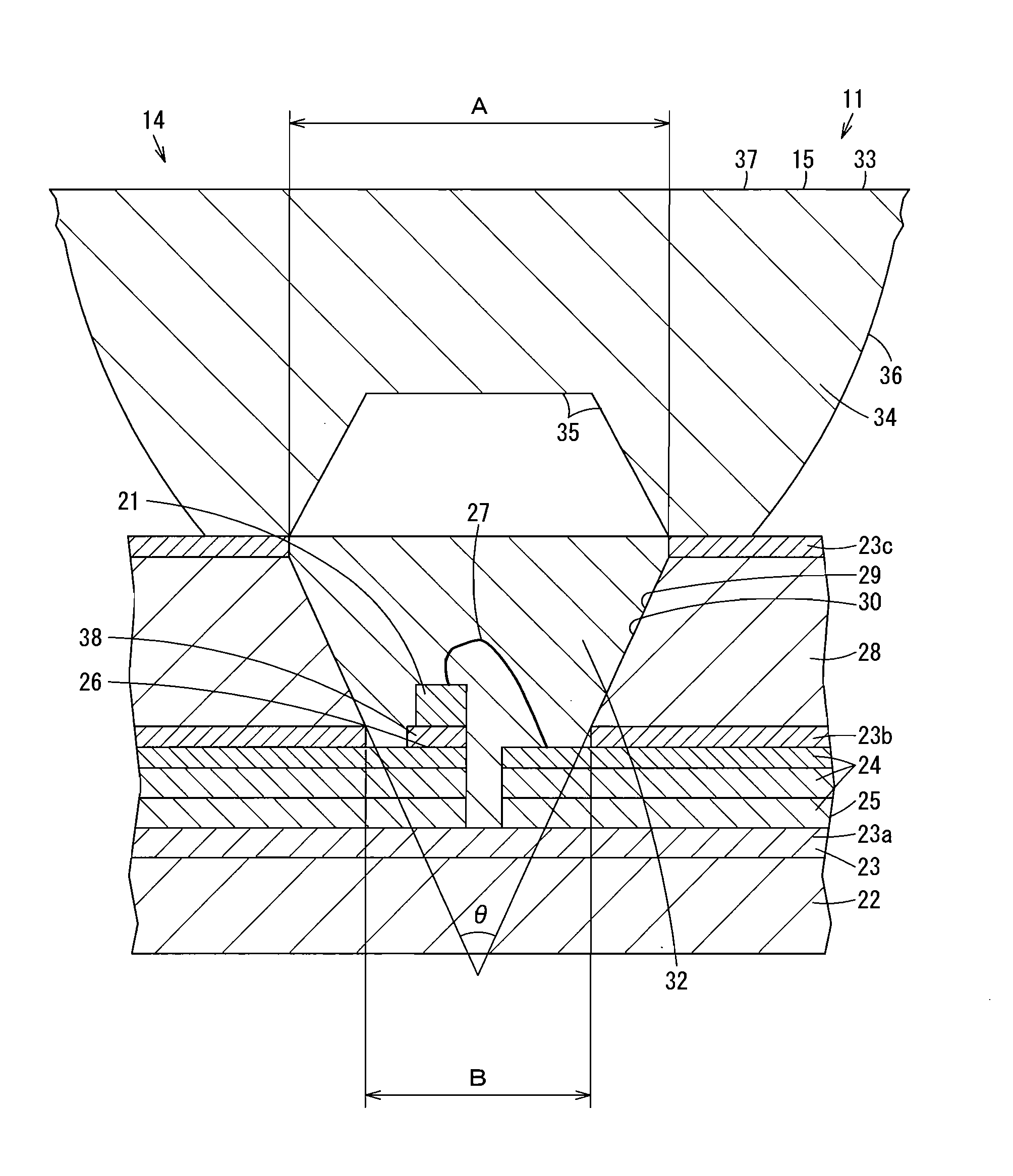
[0046]FIG. 1 to FIG. 4 show a first embodiment, with FIG. 1 being a sectional view of a light emitting module of an illuminating device, FIG. 2 being a front view of the light emitting module, FIG. 3 being a front view of the illuminating device, and FIG. 4 being an explanatory diagram of examples of combinations of materials of the light emitting module.

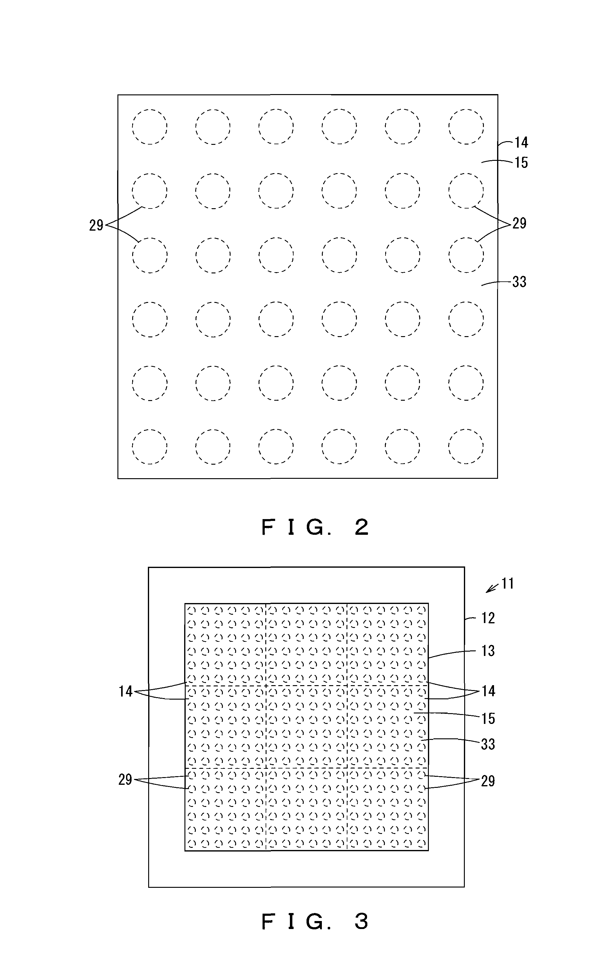
[0047]In FIG. 3, 11 is the illuminating device, and this illuminating device 11 has a thinly-formed, rectangular main device body 12, a rectangular opening 13 is formed on a surface of this main device body 12, a plurality of rectangular light emitting modules 14 are arrayed in matrix form inside the opening 13, and a light emitting surface 15 is formed by the plurality of light emitting modules 14.

[0048]As shown in FIG. 1, each light emitting module 14 has, as light emitting elements, chip type light emitting diode elements 21, which are solid-state light emitting elements, and the plurality of light emitting diode elements 21 are ...

eighth embodiment

[0088]The anchoring-portion-provided penetrating holes 62 may be arranged as tapered holes, each having a tapered shape that spreads towards the other surface side of the substrate 22, which is the side opposite the one surface side of the substrate 22 at which the reflector 28, the lens 33, etc., are disposed, as in an eighth embodiment shown in FIG. 12. In this case, the anchoring portion 63 is formed by the tapered hole itself. The tapered hole provides an action of making the resin flow in smoothly.

[0089]FIG. 13 to FIG. 16 show another embodiment. FIG. 13 is a sectional view of a portion of a light emitting module of an illuminating device, FIG. 14 is a plan view of a substrate of the illuminating device, FIG. 15 is a sectional view of the light emitting module and a main device body of the illuminating device, and FIG. 16 is a plan view of the light emitting modules and the main device body of the illuminating device.

[0090]As shown in FIG. 15 and FIG. 16, the illuminating devic...


PUM


Abstract

An illuminating device that is improved in heat radiation property and is suppressed in the occurrence of peeling and warping of a reflector. The reflector having a housing portion that houses a light emitting diode element is disposed on a substrate a visible light converting layer is formed on the housing portion and a lens is disposed on the reflector. A circuit pattern, the light emitting diode element, the reflector, the visible light converting layer, and the lens are disposed on the substrate, and the reflector and the lens are respectively adhered using a same type of adhesive agent. The heat radiation property can thus be improved, the peeling and warping of the reflector, etc., is suppressed, and accordingly, the optical characteristics of the device can be maintained.

Description

CROSS REFERENCE TO PRIOR APPLICATION[0001]This is a U.S. national phase application under 35 U.S.C. §371 of International Application No. PCT / JP2005 / 005232, filed Mar. 23, 2005 and claims the benefit of Japanese Applications No. 2004-086667, filed Mar. 24, 2004, 2004-285726, filed Sep. 30, 2004 and 2004-3473489, filed Nov. 30, 2004. The International Application was published in Japanese on Sep. 29, 2005 as International Publication No. WO 2005 / 091386 A1 under PCT Article 21(2).TECHNICAL FIELD[0002]The present invention relates to an illuminating device having a light emitting element as a light source.BACKGROUND ART[0003]Conventionally, with an illuminating device having, for example, light emitting elements, such as light emitting diode elements that are solid-state light emitting elements, as light sources, a plurality of recessed housing portions are formed on a surface of a substrate, a metal film is formed on an inner surface of each housing portion, a light emitting diode ele...

Claims


Application Information

Patent Timeline
IPC IPC(8): F21V7/00H01L33/54H01L33/58
CPCH01L33/58H01L33/54H01L2224/48091H01L2924/181H01L2224/16225H01L2224/73265H01L2224/8592H01L2924/00014H01L2924/00011H01L2924/00012H01L2224/0401
Inventor MORIYAMA, TAKAYOSHINAKANISHI, AKIKOIWAMOTO, MASAMINOGI, SHINJIOGAWA, KOZOSHIMIZU, KEIICHISAITOU, AKIKOKAWASHIMA, SEIKOSANPEI, TOMOHIROTODA, MASAHIRO
Owner TOSHIBA LIGHTING & TECH CORP
Why Eureka
Try Eureka