Method of enhancing dopant activation without suffering additional dopant diffusion

a dopant activation and diffusion technology, applied in transistors, basic electric elements, electrical equipment, etc., can solve problems such as difficult junction depth and restrict silicon device downscaling, and achieve the effect of rapid thermal anneal (rta) steps

Active Publication Date: 2008-10-02
TAIWAN SEMICON MFG CO LTD
View PDF6 Cites 17 Cited by
  • Summary
  • Abstract
  • Description
  • Claims
  • Application Information

AI Technical Summary

Benefits of technology

The present invention provides a method for activating impurities in silicon without causing additional dopant diffusion. This method involves using a flash anneal process followed by a rapid thermal anneal (RTA) step. This approach results in improved performance and reliability of MOS transistors.

Problems solved by technology

The patent text discusses the need for a better method of forming shallow junctions in semiconductor devices. The conventional method involves using ion implantation and rapid thermal annealing (RTA) to activate the dopants and remove damage. However, the use of RTA for several seconds results in additional dopant diffusion and restricts device downscaling. There is a need for a novel thermal approach that can enhance dopant activation while maintaining a low thermal budget to minimize dopant diffusion.

Method used


Image

  • Method of enhancing dopant activation without suffering additional dopant diffusion
  • Method of enhancing dopant activation without suffering additional dopant diffusion
  • Method of enhancing dopant activation without suffering additional dopant diffusion

Examples


Embodiment Construction

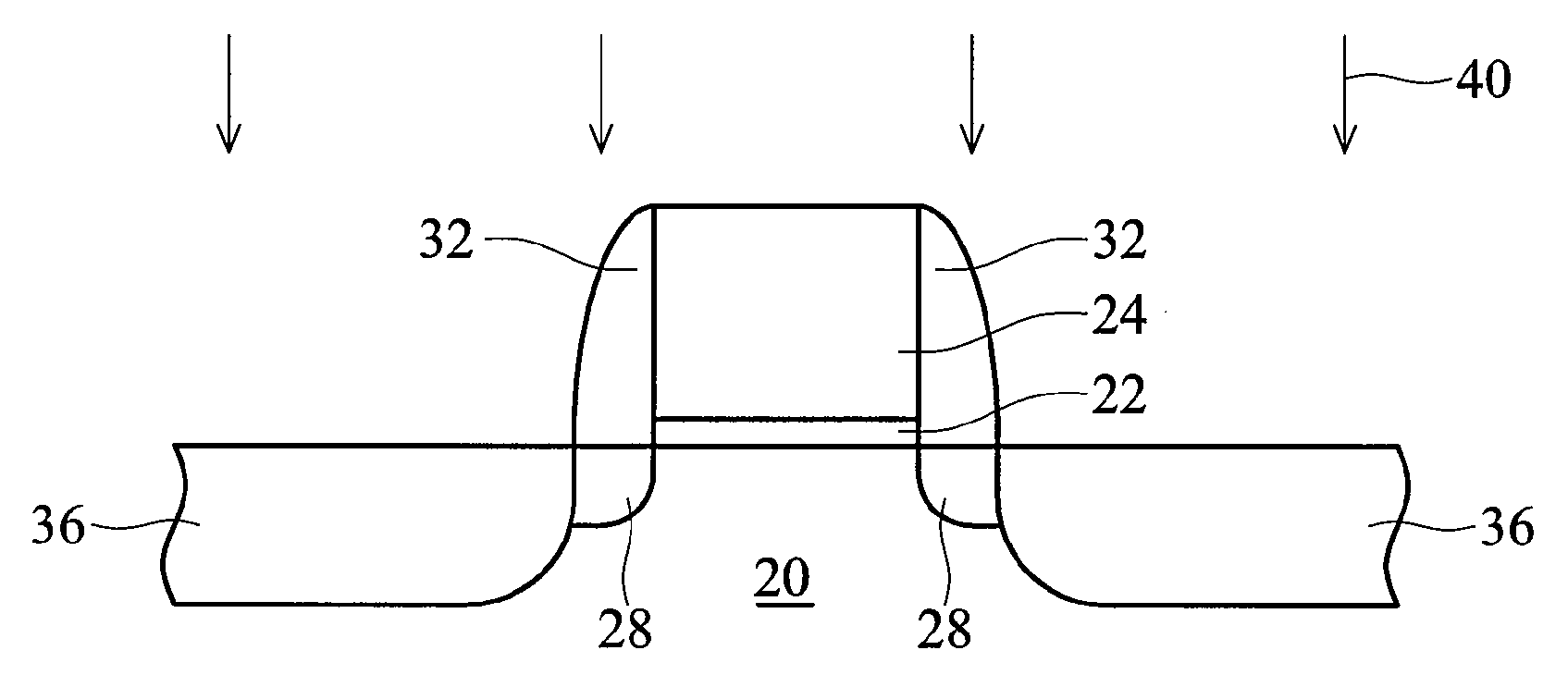
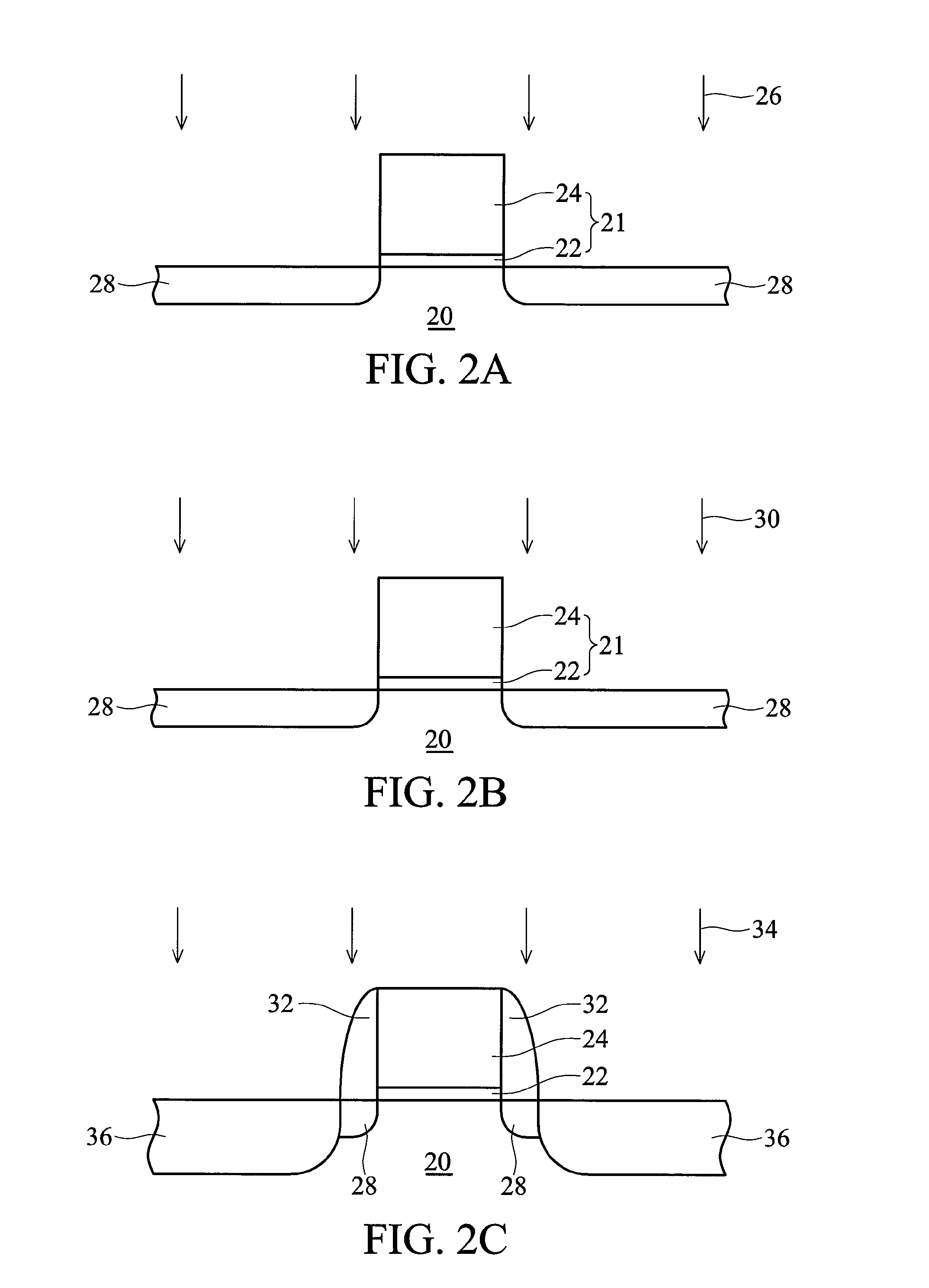
[0012]Reference will now be made in detail to the present embodiments, examples of which are illustrated in the accompanying drawings. Wherever possible, the same reference numbers are used in the drawings and the description to refer to the same or like parts. In the drawings, the shape and thickness of one embodiment may be exaggerated for clarity and convenience. This description will be directed in particular to elements forming part of, or cooperating more directly with, apparatus in accordance with the present invention. It is to be understood that elements not specifically shown or described may take various forms well known to those skilled in the art. Further, when a layer is referred to as being on another layer or “on” a substrate, it may be directly on the other layer or on the substrate, or intervening layers may also be present.

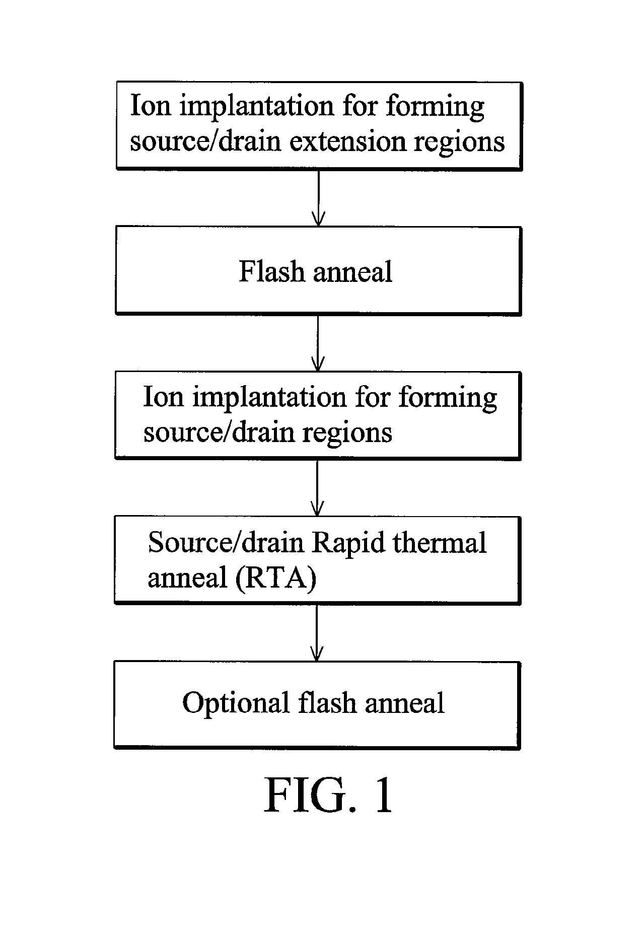
[0013]The present invention provides a thermal approach to activate impurities in silicon without suffering additional dopant diffusion. Prefer...


PUM


Abstract

A method of enhancing dopant activation without suffering additional dopant diffusion, includes forming shallow and lightly-doped source/drain extension regions in a semiconductor substrate, performing a first anneal process on the source/drain extension regions, forming deep and heavily-doped source/drain regions in the substrate adjacent to the source/drain extension regions, and performing a second anneal process on source/drain regions. The first anneal process is a flash anneal process performed for a time of between about 1 millisecond and 3 milliseconds, and the second anneal process is a rapid thermal anneal process performed for a time of between about 1 second and 30 seconds.

Description


Claims


Application Information

Patent Timeline
Owner TAIWAN SEMICON MFG CO LTD
Why Eureka
Try Eureka