Method for checking alignment accuracy using overlay mark

a technology of alignment accuracy and overlay mark, which is applied in the direction of instruments, photomechanical devices, optics, etc., can solve the problems of unreliable determining alignment accuracy between photoresist patterns, adversely affecting overlay accuracy, and unbalance stresses of the lower layer of the wafer

Inactive Publication Date: 2008-10-02
MACRONIX INT CO LTD
View PDF7 Cites 6 Cited by
  • Summary
  • Abstract
  • Description
  • Claims
  • Application Information

AI Technical Summary

Benefits of technology

[0020]Using the above method for checking the alignment of the overlay marks, the profiles and the dimensions of the alignment marks being asymmetrical can be obviated. More particularly, the error in overlay measurement accuracy resulting from a profile deformity of the exterior profile of the outer mark is mitigated. Ultimately, the results from checking alignment accuracy are desirable.

Problems solved by technology

Accordingly, the measurement of alignment accuracy, in other words, the measurement of overlay accuracy is an important issue in a semiconductor process.
However, during the fabrication of the trenches 122a, 122b, 124a, 124b as the overlay marks, the varying positions of the trenches or other factors in the fabrication process may induce unbalance stresses to the lower layer on the wafer.
The overlay shift in the X direction and the overlay shift in the Y direction adversely affect the overlay accuracy.
Hence, the conventional method is unreliable for determining alignment accuracy between the photoresist pattern and the wafer.

Method used


Image

  • Method for checking alignment accuracy using overlay mark
  • Method for checking alignment accuracy using overlay mark
  • Method for checking alignment accuracy using overlay mark

Examples


Embodiment Construction

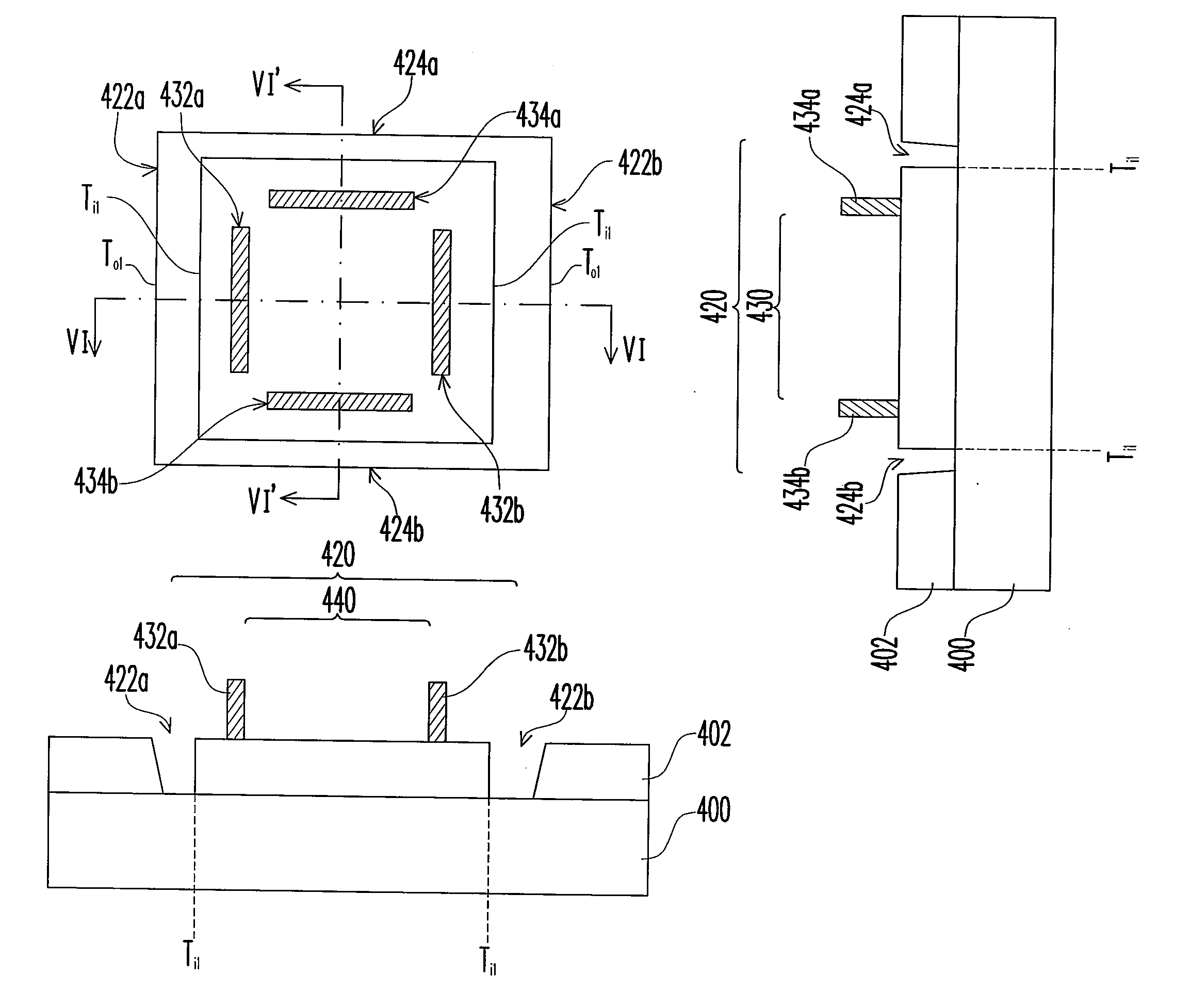
[0029]FIGS. 3, 4, and 5 are schematic diagrams respectively illustrating the overlay mark of the present invention and an application thereof. In this exemplary embodiment, the overlay mark includes, for example, two X-directional, orthogonal trenches and two Y-directional, orthogonal trenches as the outer mark, and two X-directional bars and two Y-directional bars as the inner mark. However, it is appreciated that the shapes and the configurations of the overlay mark introduced herein may be embodied in many different forms and should not be construed as limited to the embodiments set forth herein.

[0030]Referring to FIG. 3, as the lower layer 302 in the device region of a wafer 300 is being patterned, an outer mark 320 is concurrently formed in the non-device region. The outer mark 320 may constitute with, but not limited to, two Y-directional trenches 322a, 322b and two X-directional trenches 324a, 324b. Each trench also includes an exterior profile To and an interior profile Ti. ...


PUM


Abstract

A method for checking the alignment accuracy using an overlay mark is provided. The overlay mark includes an inner mark and an outer mark formed on a wafer. The outer mark is formed in a lower layer on the wafer when the lower layer is patterned. The inner mark is formed within the outer mark over the lower layer when a lithography process for defining an upper layer is performed. A measurement process is conducted to obtain a first relation between each of the interior profiles of the outer marks and a second relation between each of the inner marks. Alternatively, a third relation between each of the interior profiles of the outer marks and each of the inner marks is obtained. The X-directional alignment accuracy and y-directional alignment accuracy are computed according to the first and the second relations, or the third relation.

Description

BACKGROUND OF THE INVENTION[0001]1. Field of Invention[0002]The present invention relates to an integrated circuit (IC) fabrication process. More particularly, the present invention relates to a method for checking the alignment accuracy in a photolithograph process for defining an upper layer with respective to a lower layer on a wafer.[0003]2. Description of Related Art[0004]Generally, besides having to control the critical dimension, alignment accuracy (AA) is also an important factor for determining the success of a photolithograph process of a wafer. Accordingly, the measurement of alignment accuracy, in other words, the measurement of overlay accuracy is an important issue in a semiconductor process. Further, the overlay mark is tool for measuring an overlay error, in which the alignment between a pattern of a photoresist layer and a previously formed layer on the wafer after the lithograph process, is determined.[0005]Referring to FIG. 1, when the lower layer 102 in the devic...

Claims


Application Information

Patent Timeline
Patent Type & Authority Applications(United States)
IPC IPC(8): H01L21/70
CPCG03F7/70633
Inventor YANG, CHIN-CHENG
Owner MACRONIX INT CO LTD
Why Eureka
Try Eureka