

Means To Detect A Missing Pulse And Reduce The Associated PLL Phase Bump
a technology of phase bump and detection circuit, applied in pulse manipulation, pulse technique, instruments, etc., can solve the problems of slow response and reduced detection circuit sensitivity
- Summary
- Abstract
- Description
- Claims
- Application Information
AI Technical Summary
Problems solved by technology
Method used
Image

Examples
Embodiment Construction
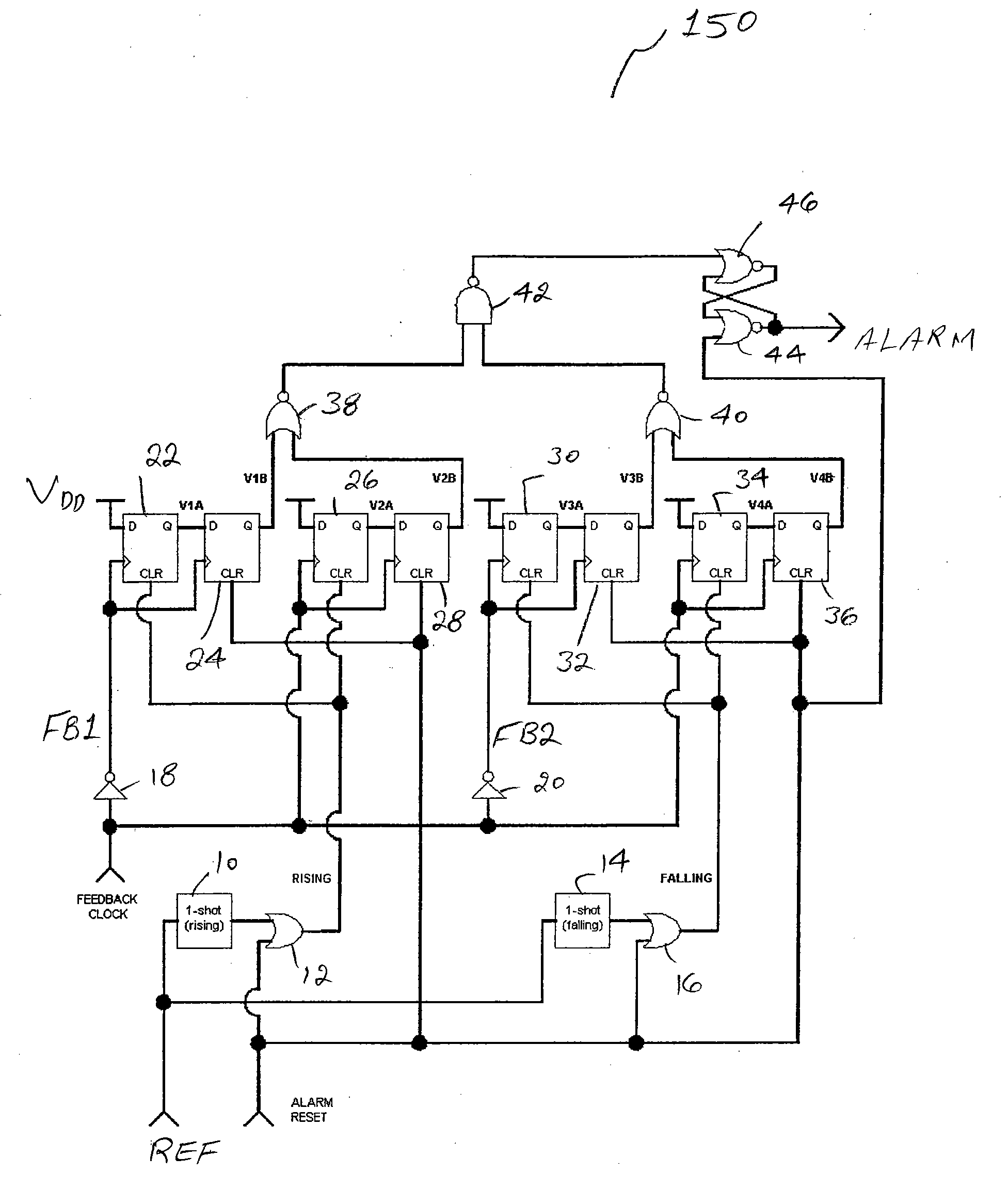
[0026]FIG. 3 is a schematic diagram of a missing pulse detection circuit 150, in accordance with one embodiment of the present invention. When a missing pulse is detected by circuit 150, the output signal Alarm of NOR gate 44 is set. Output signal ALARM is reset when signal ALARM_RESET applied to OR gate 12 is asserted.
[0027]One-shot block 10 generates a pulse on each rising edge of the reference clock signal REF and applies this pulse to OR gate 12. Likewise, one-shot block 14 generates a pulse on each falling edge of the reference clock signal REF and applies this pulse to OR gate 16. The output signal RISING of OR gate 12 is applied to the clear input terminals CLR of flip-flops 22 and 26. The output signal FALLING of OR gate 16 is applied to the clear input terminals CLR of flip-flops 30 and 34. Signal ALARM_RESET is applied to the CLR input terminals of flip-flops 24, 28, 32 and 36.
[0028]The input clock terminals of flip-flops 22 and 24 receive clock signal FB1 that is the inve...
PUM
 Abstract
Description
Claims
Application Information