Solid-state image sensing device and image sensing system

a sensing device and image technology, applied in the field of solid-state image sensing devices and image sensing systems, can solve the problems of generally large power consumption of moving image capturing, and achieve the effect of suppressing power consumption

Inactive Publication Date: 2008-11-06
CANON KK
View PDF17 Cites 70 Cited by
  • Summary
  • Abstract
  • Description
  • Claims
  • Application Information

AI Technical Summary

Benefits of technology

[0006]The present invention has been made in consideration of the above-described problems, and has as its object to suppress the power consumption in the moving image capturing mode without changing, e.g., the clock rate between the moving image capturing mode and the still image capturing mode.

Problems solved by technology

For this purpose, moving image capturing generally consumes a relatively large power.

Method used


Image

  • Solid-state image sensing device and image sensing system
  • Solid-state image sensing device and image sensing system
  • Solid-state image sensing device and image sensing system

Examples


first embodiment

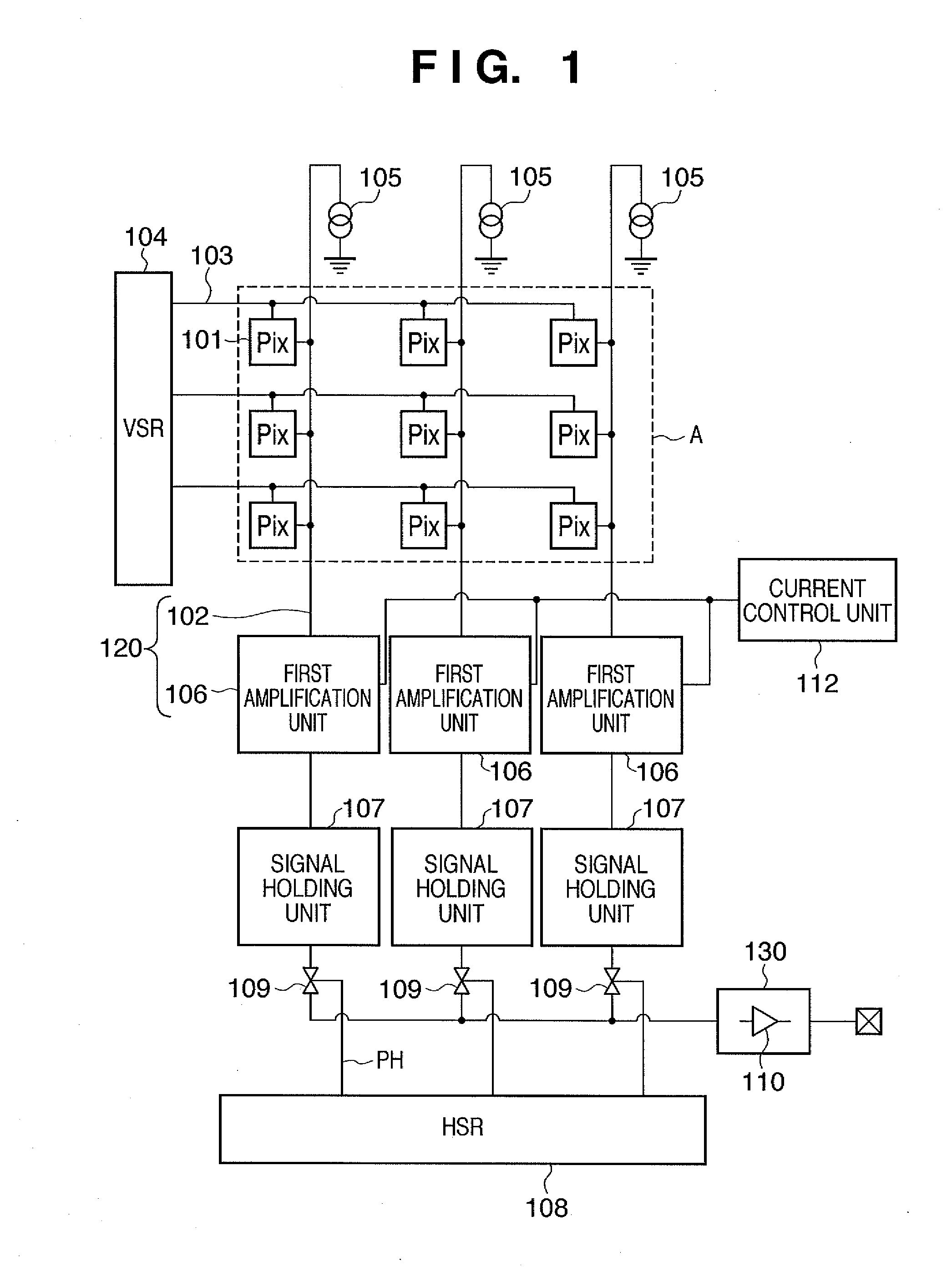
[0026]FIG. 1 is a block diagram showing the schematic arrangement of a solid-state image sensing device according to the present invention. The solid-state image sensing device comprises a pixel array A, vertical scanning circuit 104, first readout circuits (column readout circuits) 120, signal holding units 107, switches 109, horizontal scanning circuit 108, second readout circuit 130, and current control unit 112.

[0027]The pixel array A is formed by two-dimensionally arraying a plurality of pixel units 101 into a plurality of rows and a plurality of columns. For the sake of descriptive simplicity, a pixel array A is formed by 3×3 pixel units 101 in FIG. 1. However, the arrangement of the pixel array A is not particularly limited to this.

[0028]The first readout circuit 120 reads out a signal from the pixel array A, and can include, e.g., a column signal line 102, first amplification unit 106, and constant current source 105. The signal holding unit 107 holds the signal read out by ...

third embodiment

[0063]FIG. 7 is a timing chart illustrating an example of the operation of the solid-state image sensing device according to the Referring to FIG. 7, the operation in the still image capturing mode is indicated by solid lines, and the operation in the moving image capturing mode is indicated by broken lines.

[0064]The basic operation of the solid-state image sensing device according to the third embodiment is the same as that according to the first embodiment shown in FIG. 3. Mode signals PMS and / PMS are generated by the current control unit 603. The mode signal / PMS is obtained by inverting the mode signal PMS. The mode signal PMS is set at low level in the still image capturing mode, while it is set at high level in the moving image capturing mode.

[0065]In the still image capturing mode, the transistor 601 which controls the bypass route 610 is OFF, while the transistor 602 which controls the activation / deactivation of the inverting amplifier 207 is ON. Therefore, in the still im...


PUM


Abstract

A solid-state image sensing device comprises a first readout circuit configured to read out a signal from a pixel array including a plurality of pixels, a signal holding unit configured to hold the signal read out from the first readout circuit, a second readout circuit configured to read out the signal held in the signal holding unit, and a current control unit configured to control an electric current flowing through at least part of the first readout circuit while the first readout circuit reads out the signal. The current control unit controls an electric current flowing through the at least part of the first readout circuit in a moving image capturing mode to be smaller than an electric current flowing through the at least part of the first readout circuit in a still image capturing mode.

Description

BACKGROUND OF THE INVENTION[0001]1. Field of the Invention[0002]The present invention relates to a solid-state image sensing device and an image sensing system and, more particularly, to a solid-state image sensing device which can capture a moving image and a still image and an image sensing system having the same.[0003]2. Description of the Related Art[0004]A digital camera using a solid-state image sensing device which can capture both a still image and a moving image has become popular nowadays. To meet a demand for still image capturing with high image quality / high resolution, information on pixels in a number larger than that of pixels read out in moving image capturing is necessary. Although moving image capturing requires pixels fewer than those in still image capturing, a specific number of frames (e.g., 30 frames per second according to the NTSC standard) need to be recorded in one second. For this purpose, moving image capturing generally consumes a relatively large power...

Claims


Application Information

Patent Timeline
Patent Type & Authority Applications(United States)
IPC IPC(8): H04N5/225H01L27/146H04N5/335H04N5/369H04N5/374
CPCH04N5/23245H04N5/335H04N5/343H04N5/3698H04N5/378H04N5/23241H04N23/667H04N25/42H04N25/00H04N25/709H04N25/75
Inventor OKITA, AKIRAHIYAMA, HIROKIFUJIMURA, MASARU
Owner CANON KK
Why Eureka
Try Eureka