Solid-state imaging device, imaging apparatus, and electronic apparatus

a technology of solid-state imaging and imaging apparatus, which is applied in the direction of radio frequency controlled devices, instruments, television systems, etc., can solve the problems of increasing the speed of information transfer, affecting the accuracy of information transmission, so as to reduce power consumption and reduce noise. the effect of influen

Active Publication Date: 2008-11-20
SONY CORP
View PDF3 Cites 29 Cited by
  • Summary
  • Abstract
  • Description
  • Claims
  • Application Information

AI Technical Summary

Benefits of technology

[0023]According to an embodiment of the present invention, pixel information is transferred as complementary signals and reproduced by the differential amplifying unit at the post-stage. Therefore, even if noise is mixed in signals on the signal lines, the influence of the noise can be cancelled. As a result, it is possible to perform high-speed transfer.
[0024]According to another embodiment of the present invention, digital data is transferred as complementary data and reproduced by the differential amplifying unit at the post-stage. Therefore, even if noise is mixed in signals on the signal lines, the influence of the noise can be cancelled. The amplifying units are interposed between the complementary signal lines and the differential amplifying unit and the amplitude on the signal lines side is set small and the amplitude on an input side of the differential amplifying unit is set large. Therefore, the problem due to a parasitic capacitance on the horizontal signal lines as bus lines can be solved. This is because power consumption is smaller and a higher-speed transfer operation is possible in transfer of information with the small amplitude than in transfer of information with the large amplitude.

Problems solved by technology

However, when information on pixels based on image signals obtained from unit pixels is outputted to a post-stage (in general, referred to as horizontal transfer), a parasitic capacitance present in signal lines for horizontal transfer (information transfer paths: in particular, referred to as horizontal signal lines) poses a problem.
When a capacitance value of the parasitic capacitance increases, the parasitic capacitance is more likely to cause a signal delay and prevents an increase in speed of information transfer.
This limits a high-speed operation particularly requested in recent years.

Method used


Image

  • Solid-state imaging device, imaging apparatus, and electronic apparatus
  • Solid-state imaging device, imaging apparatus, and electronic apparatus
  • Solid-state imaging device, imaging apparatus, and electronic apparatus

Examples


Embodiment Construction

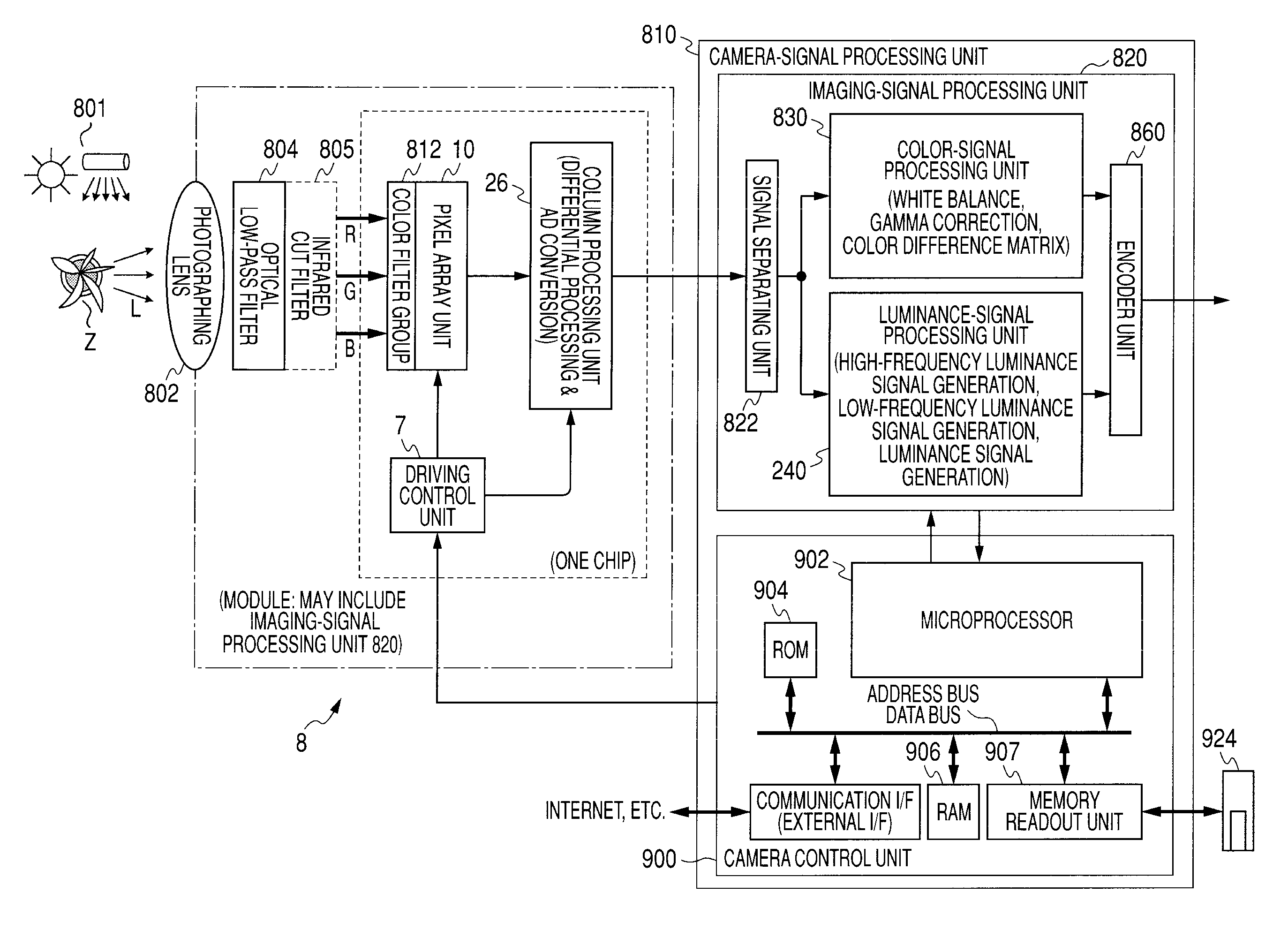
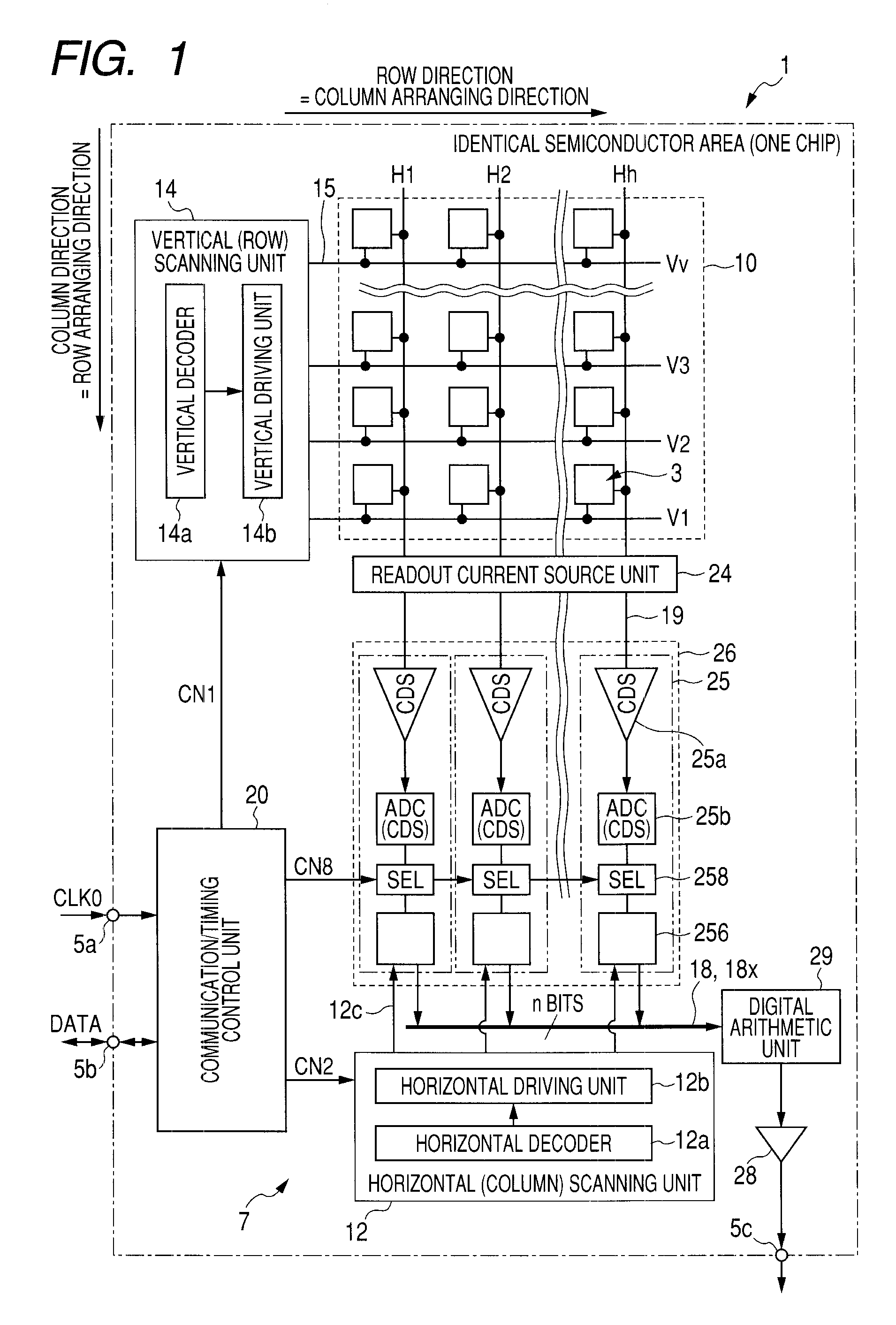
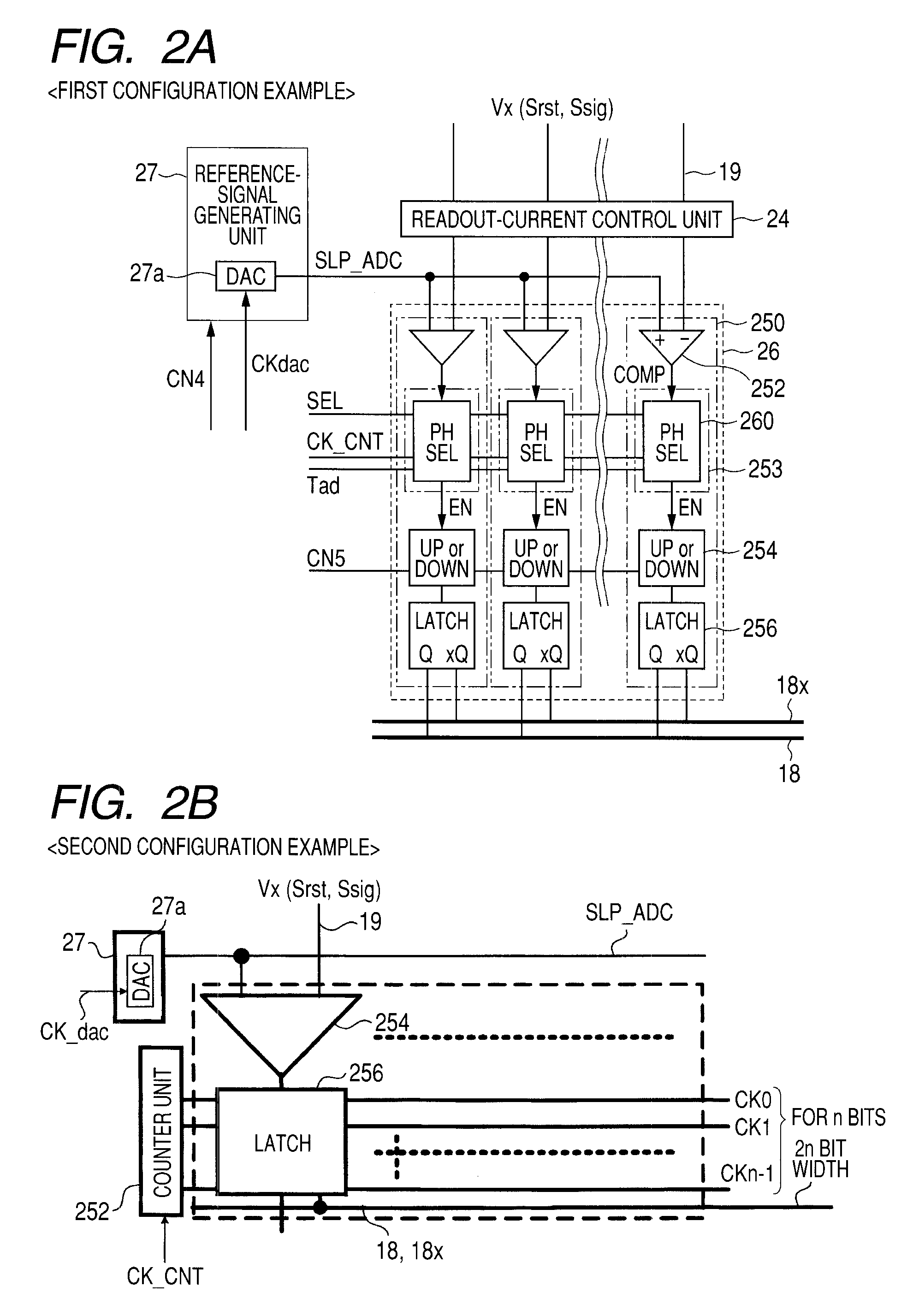
[0042]Embodiments of the present invention will be hereinafter explained with reference to the accompanying drawings. In an example explained below, a CMOS solid-state imaging device, which is an example of a solid-state imaging device of an X-Y address type, is used as a device. It is assumed that all pixels of the CMOS solid-state imaging device are formed by NMOSs.

[0043]However, this is only an example. A devise to be used is not limited to a solid-state imaging device of a MOS type. All the embodiments described later can be applied in the same manner to all semiconductor devices for detecting a physical quantity distribution formed by arraying plural unit elements, which have sensitivity to the an electromagnetic wave inputted from the outside such as light or a radiation, in a line shape or a matrix shape

[0044]FIG. 1 is a schematic diagram of a CMOS solid-state imaging device (a CMOS image sensor) as a solid-state imaging device according to an embodiment of the present invent...


PUM


Abstract

A solid-state imaging device includes a pixel unit in which unit pixels are arrayed, a complementary-signal generating unit that generates two kinds of complementary signals having complementarity with each other on the basis of analog pixel signals read out from the respective unit pixels in the pixel unit, two kinds of complementary signal lines on which the two kinds of complementary signals are transmitted, a horizontal scanning unit that transfers each of the two kinds of complementary signals on the complementary signal lines, and a differential amplifying unit that receives the signals on the two kinds of complementary signal lines with differential inputs and compares the signals.

Description

CROSS-REFERENCES TO RELATED APPLICATIONS[0001]The present invention contains subject matter related to Japanese Patent Application JP 2007-132787 filed in the Japanese Patent Office on May 18, 2007, the entire contents of which being incorporated herein by reference.BACKGROUND OF THE INVENTION[0002]1. Field of the Invention[0003]The present invention relates to a solid-state imaging device that is an example of an semiconductor device for detecting a physical quantity distribution, an imaging apparatus, and an electronic apparatus, and, more particularly to a mechanism that sequentially outputs signals to other function units and to the outside (e.g., by horizontally transferring the signals).[0004]2. Description of the Related Art[0005]In the field of electric circuits, electric signals generated by a certain function unit are often sequentially transferred to other function units and to the outside (e.g., by horizontal transfer).[0006]For example, a physical quantity distribution ...

Claims


Application Information

Patent Timeline
Patent Type & Authority Applications(United States)
IPC IPC(8): H04N5/335H01L27/146H04N5/374H04N5/378
CPCH04N3/1512H04N3/155H04N5/37455H04N5/3575H04N5/335G06V40/1318H04N25/00H04N25/616H04N25/772H04N25/75H04N25/77
Inventor TAURA, TADAYUKI
Owner SONY CORP
Why Eureka
Try Eureka