

Stage yield prediction
a technology of stage yield and product yield, applied in the direction of cad techniques, stochastic cad, instruments, etc., can solve the problems of defective integrated circuits, circuit defects, and extremely complex process of integrated circuit fabrication
- Summary
- Abstract
- Description
- Claims
- Application Information
AI Technical Summary
Benefits of technology
Problems solved by technology
Method used
Image

Examples
Embodiment Construction
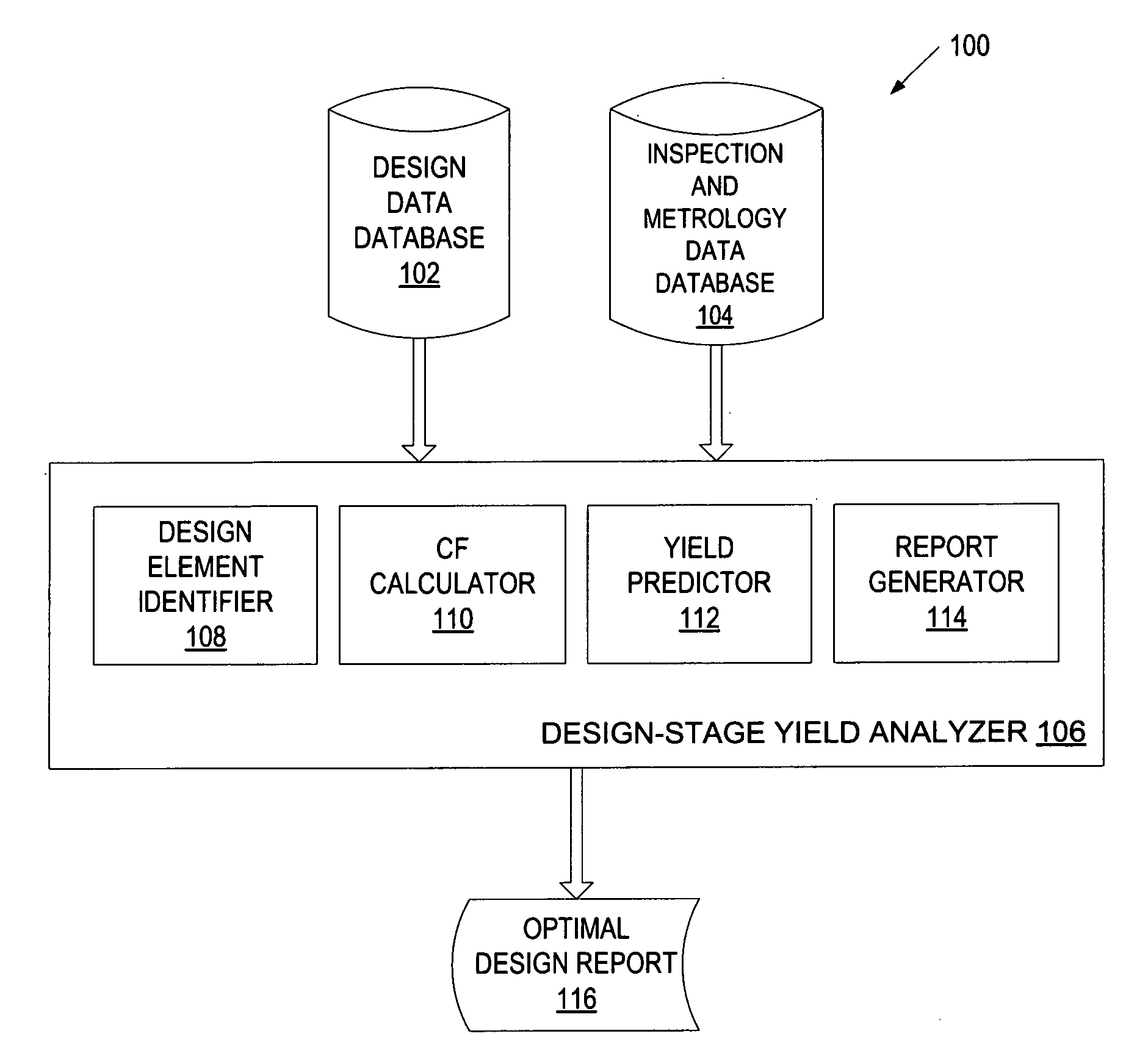
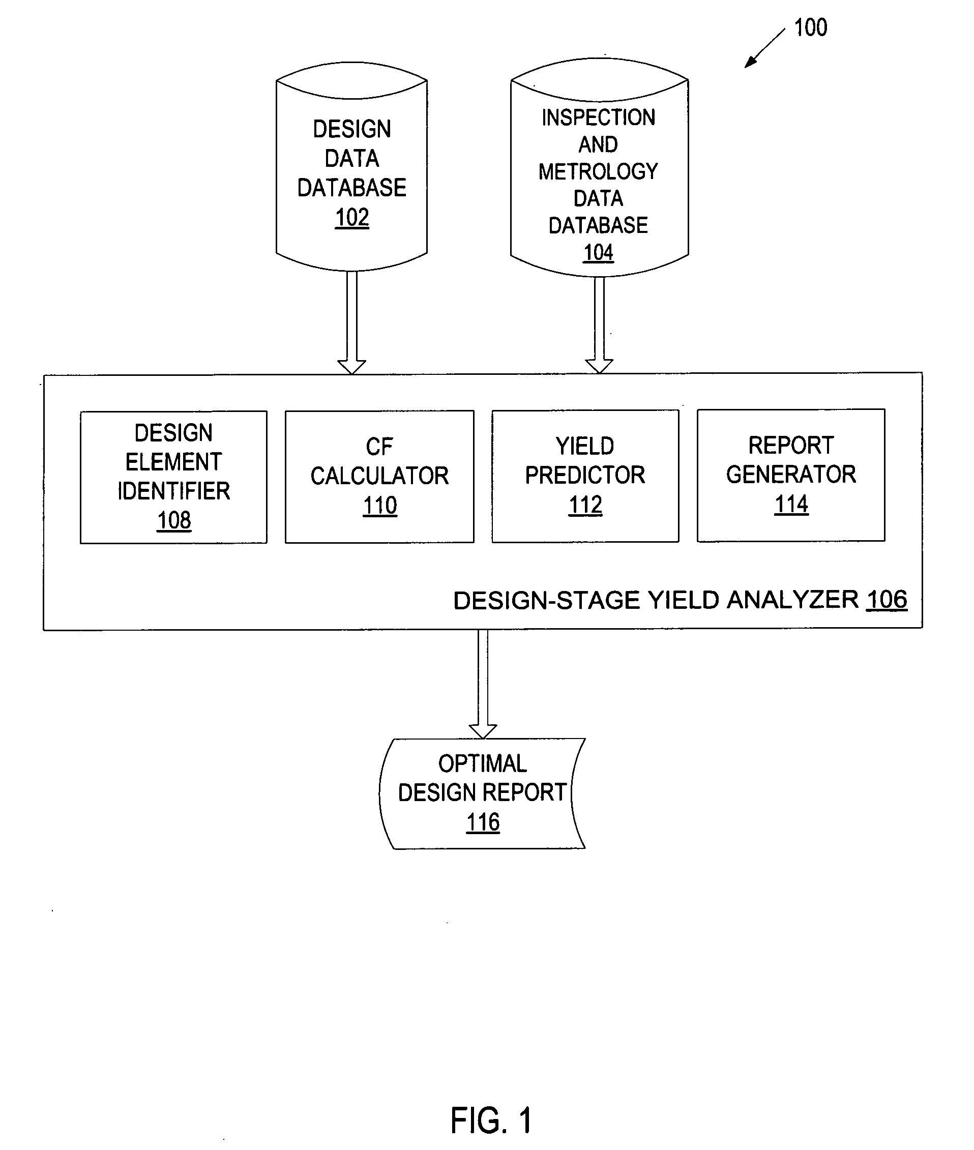
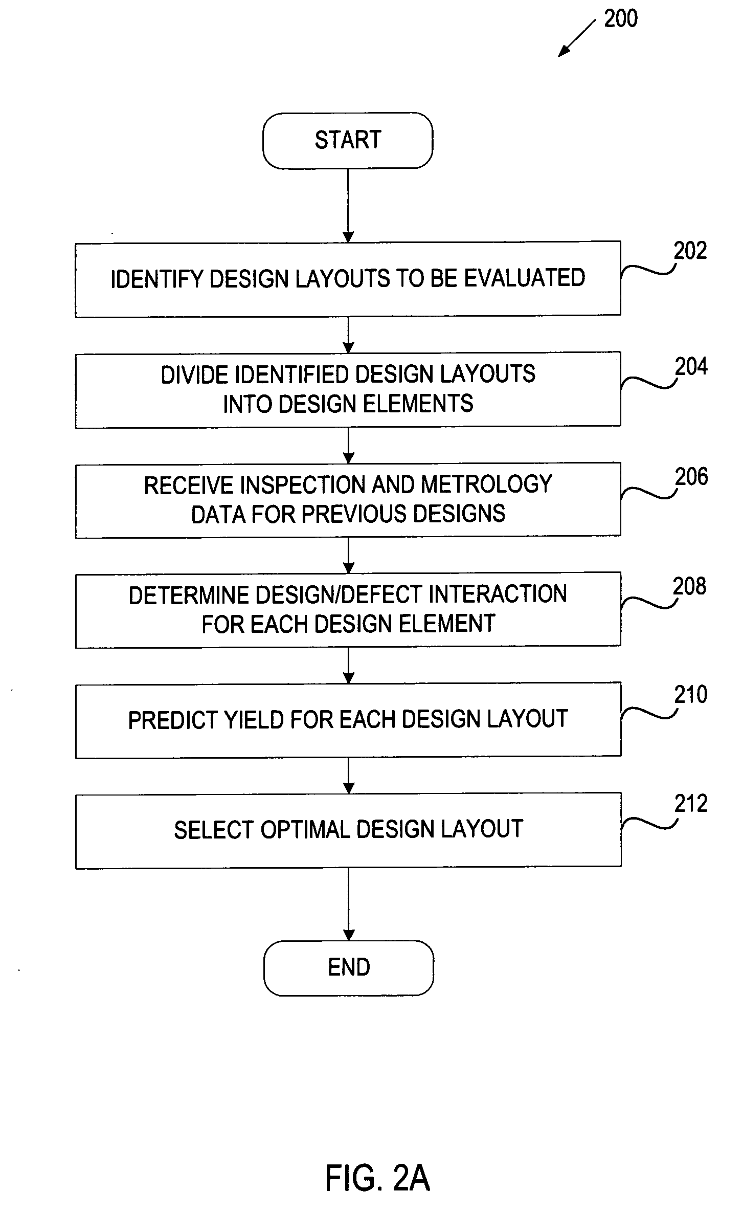
[0018]Embodiments of the invention provide a method and apparatus for predicting yield during the design stage. Using inspection data identifying defects associated with previous wafer designs (i.e., existing wafer designs previously used), defects are divided into systematic defects and random defects. For each design layout, yield is predicted separately for the systematic defects and random defects. A designer can then use the combined yield to select an optimal new design layout.
[0019]Some portions of the detailed description which follows are presented in terms of algorithms and symbolic representations of operations on data bits within a computer memory. These algorithmic descriptions and representations are the means used by those skilled in the data processing arts to most effectively convey the substance of their work to others skilled in the art. An algorithm is here, and generally, conceived to be a self-consistent sequence of steps leading to a desired result. The steps ...
PUM
 Abstract
Description
Claims
Application Information