Apparatus and method for thermally treating semiconductor device capable of preventing wafer from warping

a technology of thermal treatment and semiconductor devices, which is applied in the direction of baking ovens, lighting and heating apparatus, ovens, etc., can solve the problem of large gas flow rate on the section of the wafer with severe warping, and achieve the effect of preventing the warping of the wafer

Inactive Publication Date: 2008-12-04
SK HYNIX INC
View PDF13 Cites 27 Cited by
  • Summary
  • Abstract
  • Description
  • Claims
  • Application Information

AI Technical Summary

Benefits of technology

[0008]The present invention provides a thermal treatment apparatus capable of...

Problems solved by technology

The injecting of the reactant gas into the process chamber makes t...

Method used


Image

  • Apparatus and method for thermally treating semiconductor device capable of preventing wafer from warping
  • Apparatus and method for thermally treating semiconductor device capable of preventing wafer from warping
  • Apparatus and method for thermally treating semiconductor device capable of preventing wafer from warping

Examples


Embodiment Construction

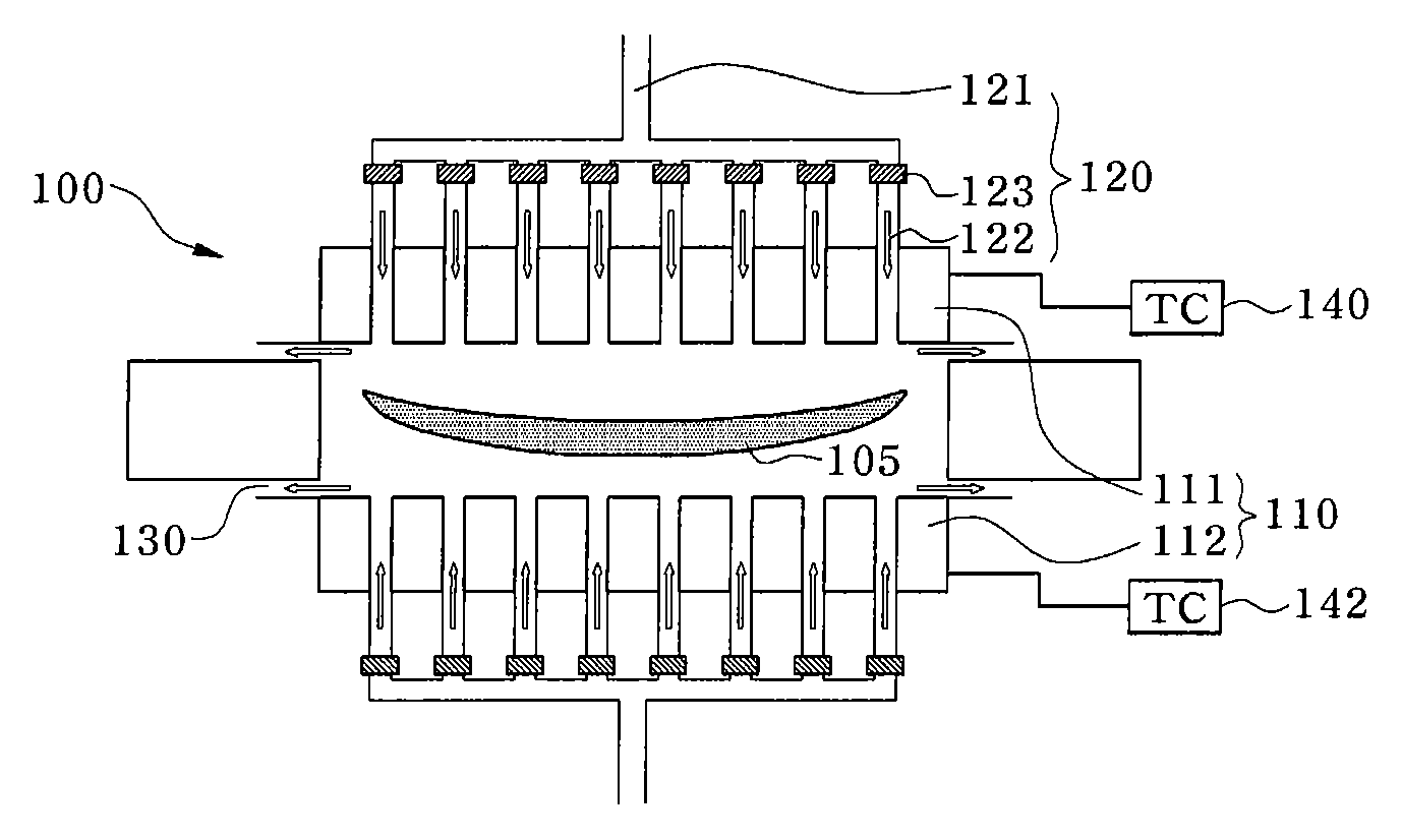
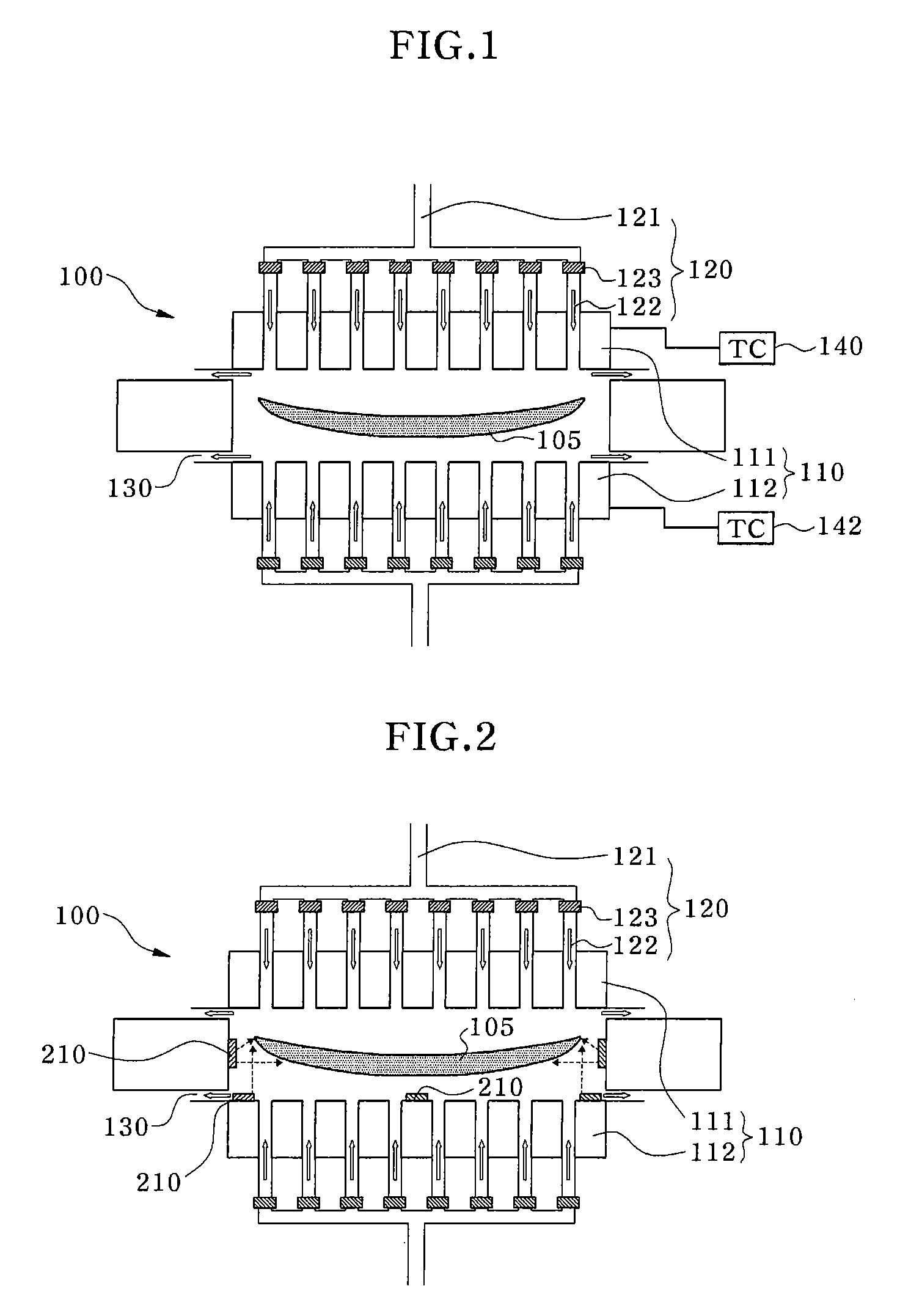
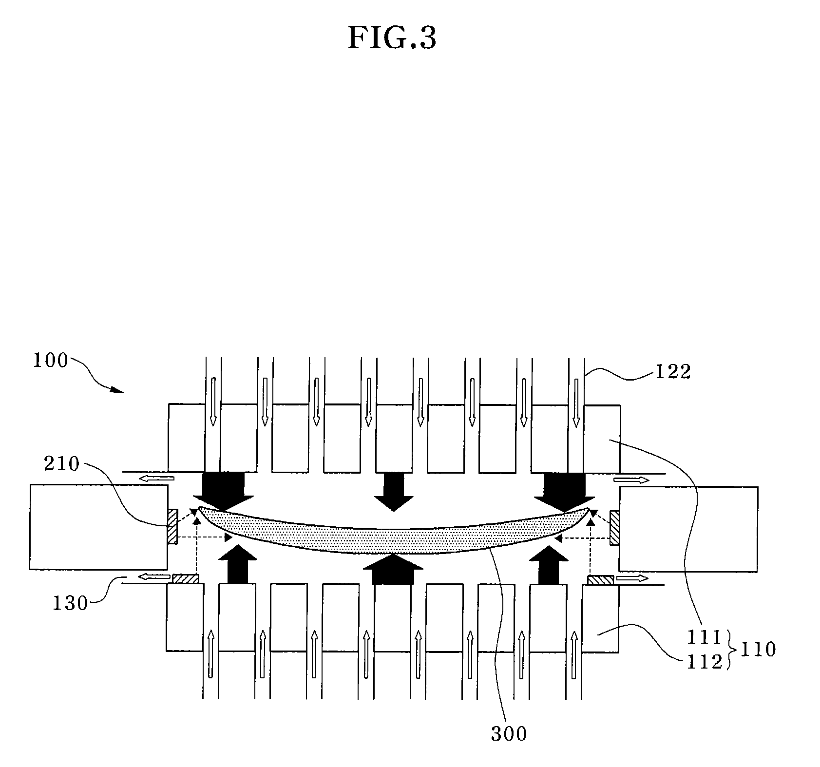
[0014]FIG. 1 is a schematic view which shows a thermal treatment apparatus where a wafer warped upwardly is loaded according to one embodiment of the present invention.

[0015]In one embodiment, a thermal treatment apparatus may include a process chamber 100 providing a space for thermally treating a wafer 105, a heating unit 110 having a plurality of heater blocks 111 and 112 to provide a predetermined temperature for the wafer 105 loaded in the process chamber 100, a gas supply unit 120 having a plurality of gas inlets 122 for supplying a reactant gas and a purge gas to the wafer 105 loaded in the process chamber, and a gas exhaust unit (not shown) having a plurality of gas outlets 130 for exhausting the reactant gas and the purge gas supplied to the process chamber in which the wafer 105 is loaded. Although not shown in FIG. 1, a wafer loading unit is established in the process chamber 100 for loading or unloading a wafer which undergoes the thermal treatment.

[0016]As shown in FIG....


PUM


Abstract

A thermal treatment apparatus and method for processing a wafer are provided. The thermal treatment apparatus includes a process chamber for thermally treating the wafer, a heating unit for heating the wafer in the process chamber, and a gas supply unit for supplying a gas and controlling a gas pressure differently by sections of the wafer. The heating unit is provided in at least one of the upper side and the lower side of the process chamber. The heating unit includes a plurality of heater blocks capable of controlling a temperature for sections of the wafer.

Description

CROSS-REFERENCES TO RELATED APPLICATIONS[0001]The present application claims priority to Korean application number 10-2007-0051528, filed on May 28, 2007, which is incorporated by reference in its entirety.BACKGROUND OF THE INVENTION[0002]The present invention relates to an apparatus and a method for fabricating a semiconductor device; and more particularly, to a thermal treatment apparatus capable of preventing a wafer from warping and a thermal treatment method using the apparatus.[0003]In the process of fabricating a semiconductor device, thermal treatment is essential. Thermal treatment is used in the process of fabricating a semiconductor device for various reasons. For example, in case of oxidizing a silicon wafer, making it into a silicon oxide film (SiO2) and using it as an insulation layer, an etching mask or a gate oxide film of a transistor, thermal treatment is used for an annealing process of thin films and a reflow process for planarizing flowable films like a Boro-Pho...

Claims


Application Information

Patent Timeline
IPC IPC(8): H01L21/324F27D11/00F27D9/00
CPCH01L21/67109H01L21/67288H01L21/6838H01L21/324
Inventor JIN, SEUNG WOOROUH, KYOUNG BONG
Owner SK HYNIX INC
Why Eureka
Try Eureka