Semiconductor laser device

a laser device and semiconductor technology, applied in semiconductor lasers, laser details, electrical equipment, etc., can solve the problems of disadvantageous presence of strong peak (substrat mode) and disadvantageous light leakage from the waveguide of the semiconductor layer to a side of the substra

Inactive Publication Date: 2009-01-29
SANYO ELECTRIC CO LTD
View PDF25 Cites 44 Cited by
  • Summary
  • Abstract
  • Description
  • Claims
  • Application Information

AI Technical Summary

Problems solved by technology

In the semiconductor laser device, it is known that light disadvantageously leaks from the waveguide of the semiconductor layer to a side of the substrate.
In the conventional semiconductor laser device disclosed in Japanese Patent Laying-Open No.

Method used


Image

  • Semiconductor laser device
  • Semiconductor laser device
  • Semiconductor laser device

Examples


first embodiment

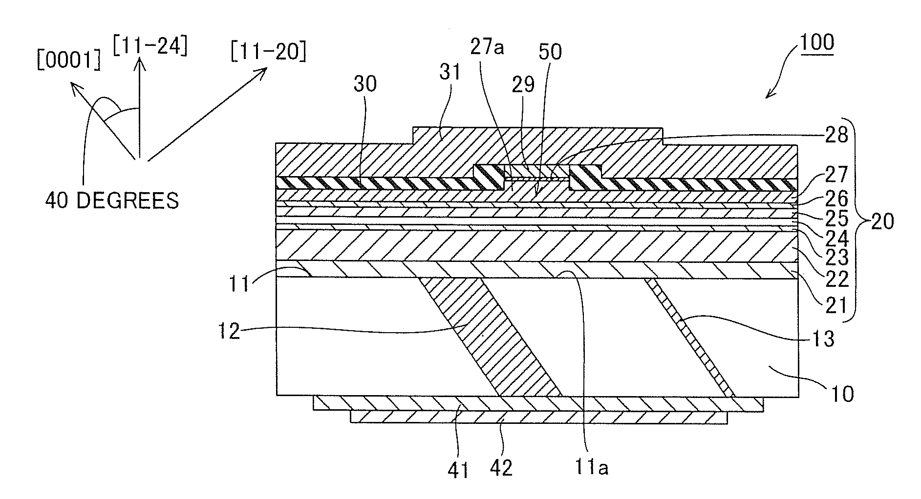
[0025]A structure of a semiconductor laser device 100 according to a first embodiment will be now described with reference to FIG. 1.

[0026]As shown in FIG. 1, the semiconductor laser device 100 according to the first embodiment is a laser device emitting a blue-violet laser of 405 nm and comprises a substrate 10, a semiconductor layer 20, a p-side ohmic electrode 29, current blocking layers 30, a p-side pad electrode 31, an n-side ohmic electrode 41 and an n-side pad electrode 42.

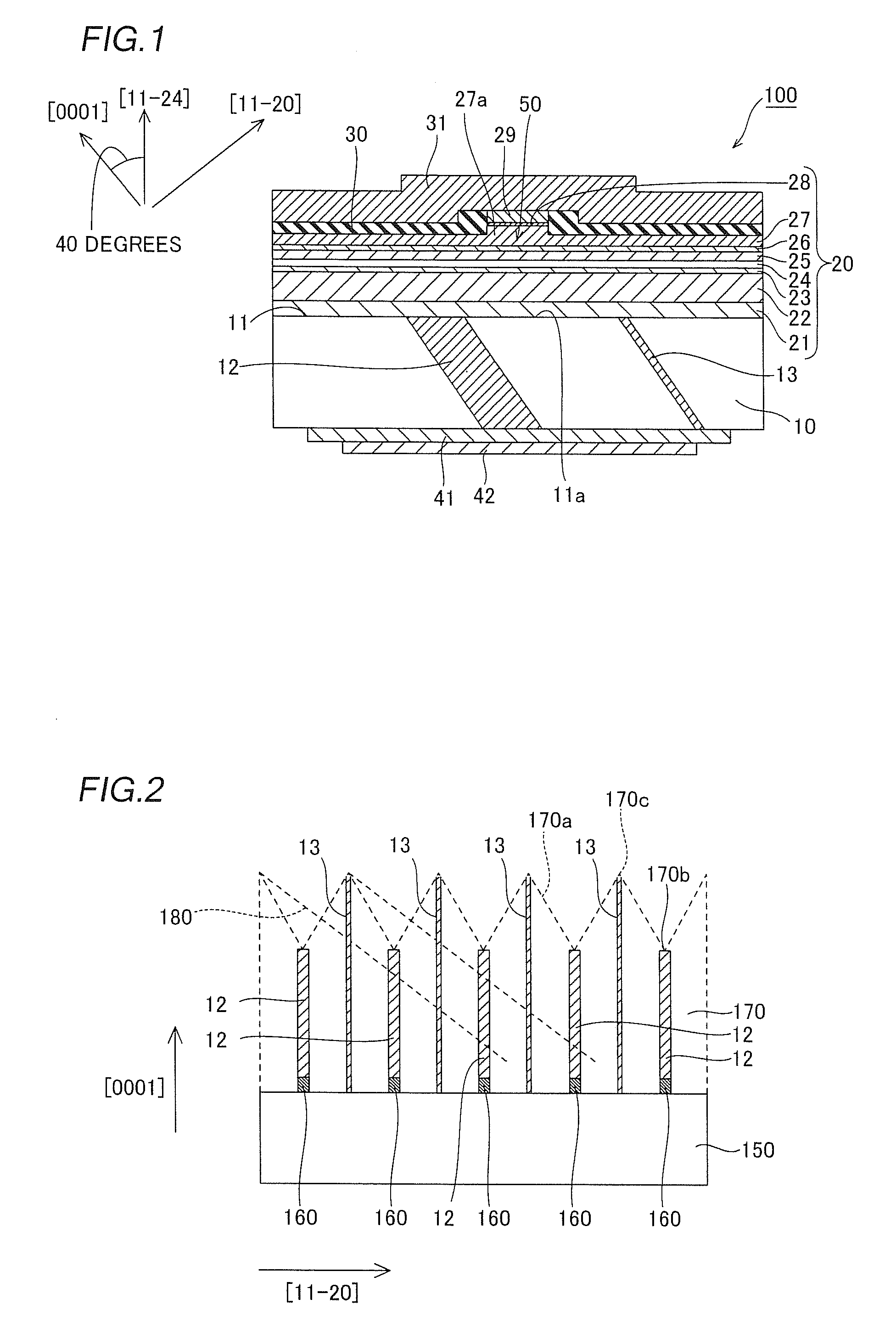
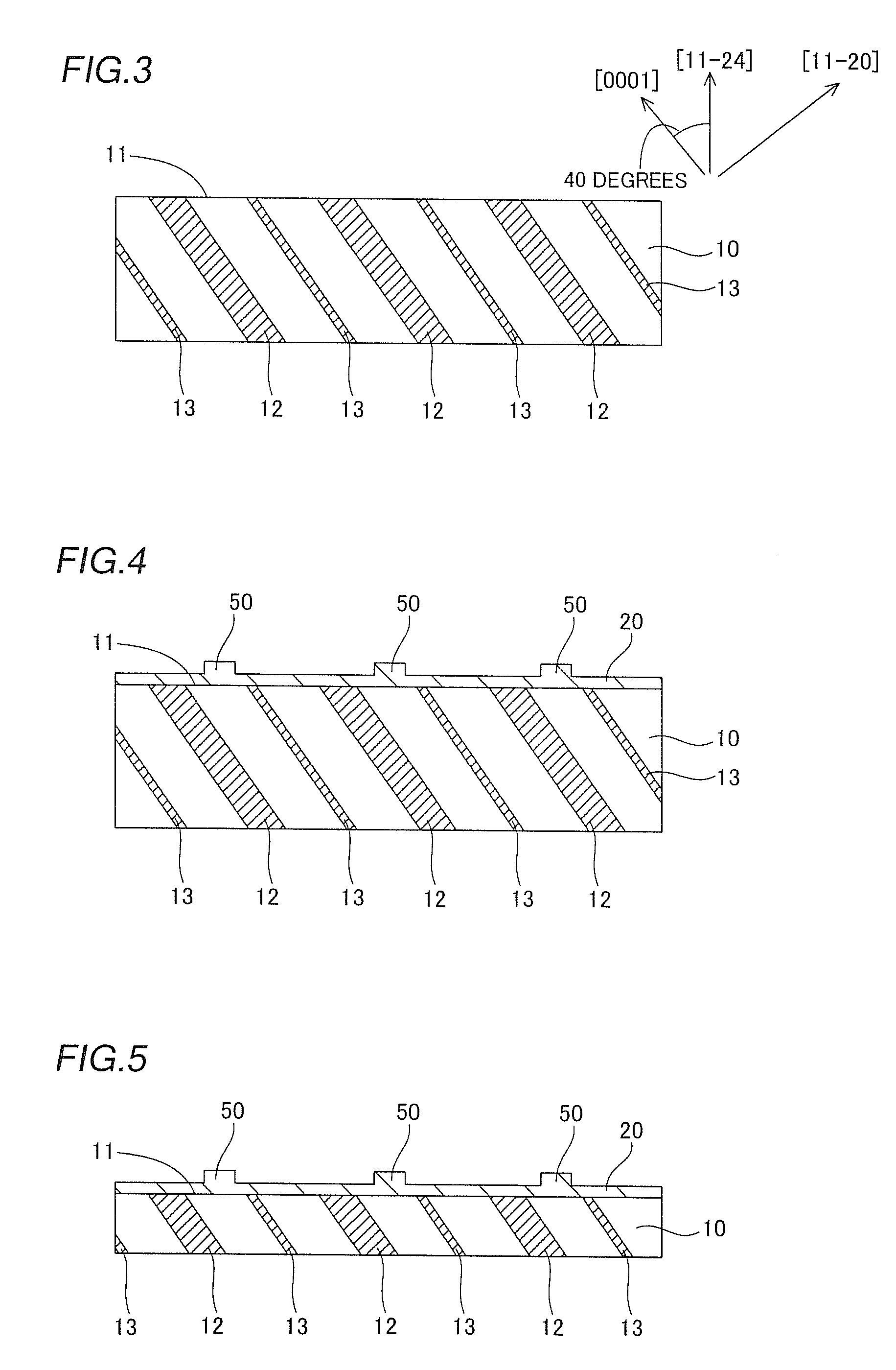
[0027]The substrate 10 is made of n-type GaN and has a thickness of about 100 μm. According to the first embodiment, a principal surface 11 of the substrate 10 is substantially equal to a (11-24) plane. In the substrate 10, a planar dislocation concentrated region 12 and a high resistance region 13 are so arranged as to extend parallel to a (11-20) plane. The dislocation concentrated region 12 and the high resistance region 13 are inclined by about 50 degrees with respect to the principal surface 11 of the ...

second embodiment

[0068]Referring to FIG. 11, a substrate is sliced along a (10-10) plane in a second embodiment dissimilar to the aforementioned first embodiment in which the substrate is sliced along the plan inclined from the (0001) plane to the [11-10] direction by about 40 degrees. In this second embodiment, the present invention is applied to a green semiconductor laser dissimilarly to the aforementioned first embodiment in which the present invention is applied to the blue-violet semiconductor laser.

[0069]As shown in FIG. 11, a semiconductor laser device 400 according to the second embodiment comprises a substrate 410, a semiconductor layer 420, a p-side ohmic electrode 29, current blocking layers 30, a p-side pad electrode 31, an n-side ohmic electrode 41 and an n-side pad electrode 42.

[0070]The substrate 410 is made of n-type GaN and has a thickness of about 100 μm. According to the second embodiment, a principal surface 411 of the substrate 410 is substantially equal to the (10-10) plane. I...


PUM


Abstract

A semiconductor laser device includes a substrate made of a nitride-based semiconductor and a waveguide formed on a principal surface of the substrate, wherein the substrate includes a dislocation concentrated region arranged so as to obliquely extend with respect to the principal surface of the substrate, and the waveguide is so formed as to be located above the dislocation concentrated region and also located on a region except a portion where the dislocation concentrated region is present in the principal surface of the substrate.

Description

CROSS-REFERENCE TO RELATED APPLICATIONS[0001]The priority application number JP2007-191812, Semiconductor Laser Device, Jul. 24, 2007, Ryoji Hiroyama et al, upon which this patent application is based is hereby incorporated by reference.BACKGROUND OF THE INVENTION[0002]1. Field of the Invention[0003]The present invention relates to a semiconductor laser device, and more particularly, it relates to a semiconductor laser device comprising a substrate made of a nitride-based semiconductor.[0004]2. Description of the Background Art[0005]A semiconductor laser device comprising a substrate made of nitride is known in general, as disclosed in Japanese Patent Laying-Open Nos. 2003-133649 and 2002-29897, for example.[0006]The aforementioned Japanese Patent Laying-Open No. 2003-133649 discloses a semiconductor laser device provided with a semiconductor layer including a waveguide on a substrate including a dislocation concentrated region extending in a direction perpendicular to a principal s...

Claims


Application Information

Patent Timeline
IPC IPC(8): H01S5/026
CPCB82Y20/00H01S5/0206H01S2301/173H01S5/3202H01S5/34333H01S5/2201H01S5/0202H01S5/0217H01S5/320275
Inventor HIROYAMA, RYOJINOMURA, YASUHIKOHATA, MASAYUKIMIYAKE, YASUTO
Owner SANYO ELECTRIC CO LTD
Why Eureka
Try Eureka