Method and structure for textured thermal cut for photovoltaic applications for thin films
Inactive Publication Date: 2009-03-12
SILICON CHINA HK
View PDF2 Cites 0 Cited by
Summary
Abstract
Description
Claims
Application Information
AI Technical Summary
This helps you quickly interpret patents by identifying the three key elements:
Problems solved by technology
Method used
Benefits of technology
Benefits of technology
[0012]Many benefits are achieved by way of the present invention over conventional techniques. For example, the present technique provides an easy to use process that relies upon conventional technology such as silicon materials, although other materials can also be used. Additionally, the method provides a process that is compatible with conventional process technology without substantial modifications to conventional equipment and processes. Preferably, the invention provides for an improved solar cell, which is less costly and easy to handle. Such solar cell uses a hydrogen co-implant to form a thin layer of photovoltaic material. Since the layers are very thin, multiple layers of photovoltaic
Problems solved by technology
Greenhouse gases are evolving a rapid rate, leading to global warming.
As the population of the world increases rapidly to over six billion people, there has been an equally large consumption of energy resources, which leads to additional greenhouse gases.
As merely an example, further increases in oil consumption have been projected.
Oil is becoming increasingly scarce.
Unfortunately, solar c
Method used
Image
Click on the blue label to locate the original text in one second.
Reading with bidirectional positioning of images and text.
Examples
embodiment
General Method Embodiment
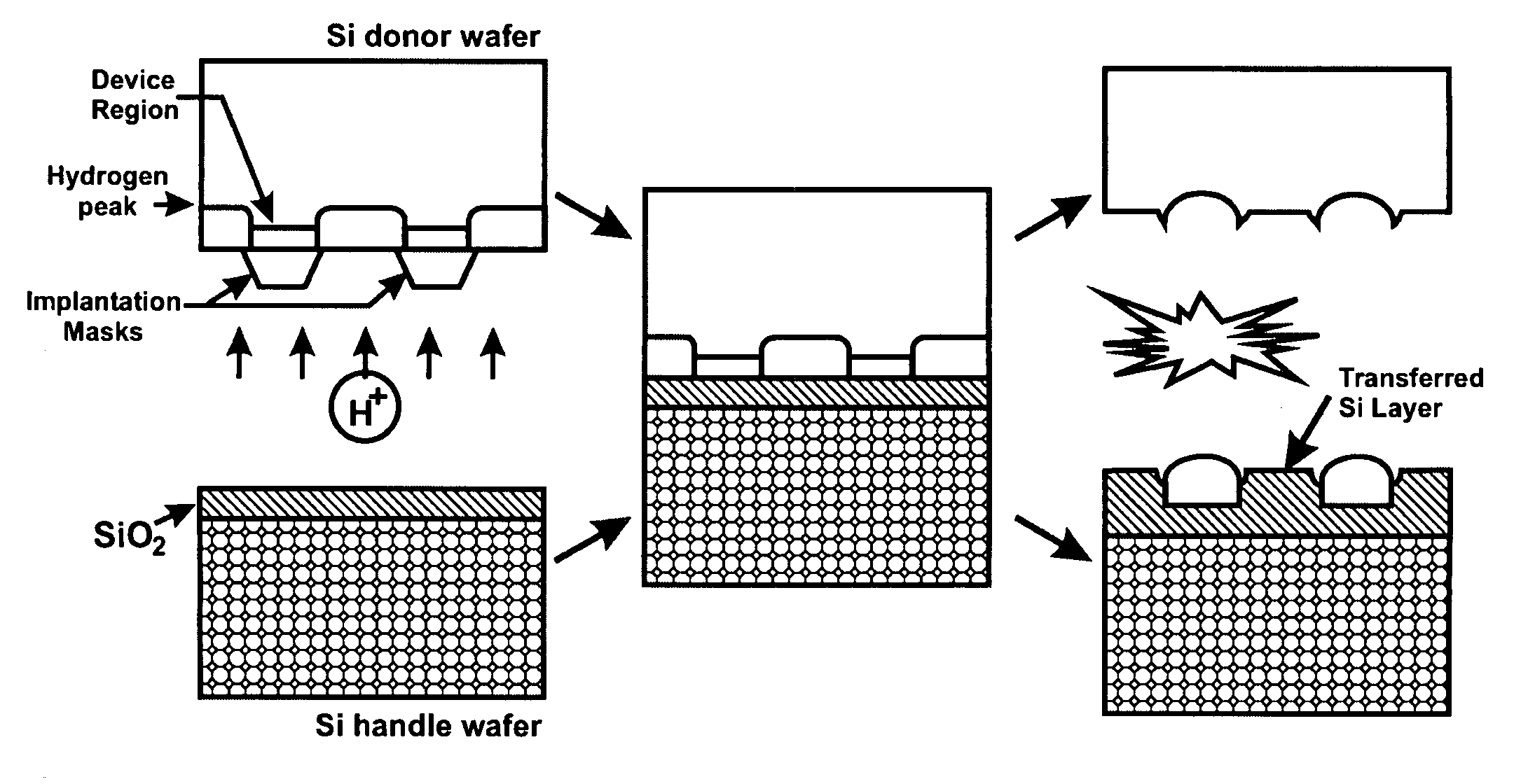
[0017]In a specific embodiment, the present invention provides a method for fabricating a photovoltaic device that can be outlined as follows:
[0018]1. Provide a semiconductor substrate, e.g., single crystal silicon, silicon germanium, Group II / VI, Group III / V;
[0019]2. Form a blocking layer (e.g., mask, block, photo mask) including a plurality of opened regions overlying the surface region of the semiconductor substrate;
[0020]3. Forming a patterned cleave region using an co-implant process including hydrogen species by subjecting at least the hydrogen species to the plurality of opened regions to define a thickness of material to be detached, which is provided between the surface region and the patterned cleave region;
[0021]4. Remove the blocking layer;
[0022]5. Join the surface region of the semiconductor substrate via a glue layer to a support surface region of a support substrate;
[0023]6. Delaminate the thickness of material from a remaining portion of the ...
examples
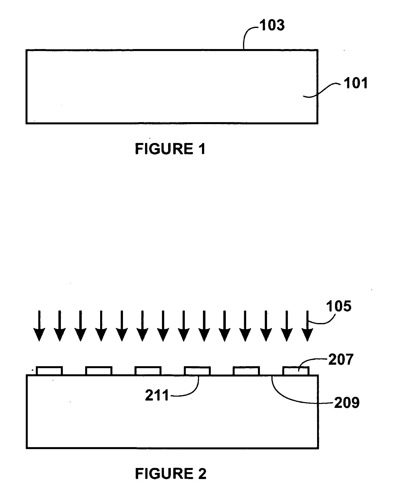
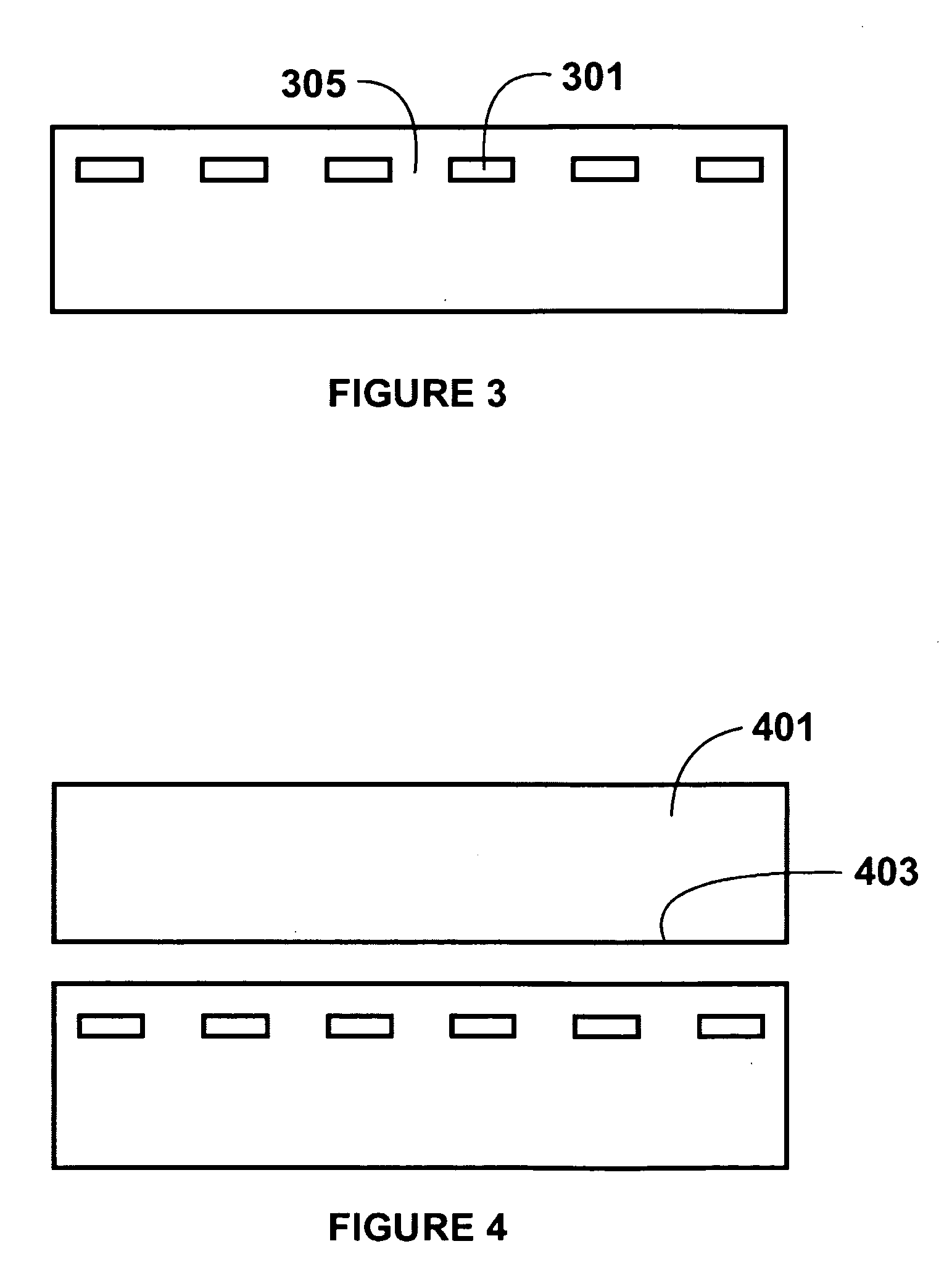
[0047]To prove the principles and operation of the present invention, we have performed experiments. These experiments are merely examples, which should not unduly limit the scope of the claims herein. One of ordinary skill in the art would recognize many variations, modifications, and alternatives. These experiments are merely for purposes of demonstrating the texturing process in accordance with the present invention. Referring To FIG. 9, we have provided a simplified set of diagrams illustrating our experiment.
[0048]As shown, we provided a method for fabricating a photovoltaic material. As shown, the method includes providing a single crystal silicon semiconductor substrate, which includes surface region. The substrate included a blocking layer overlying the surface region. In a specific embodiment, the blocking layer was photosensitive material that included a plurality of opened regions. Such opened regions are separated by blocking layer according to a specific embodiment. We ...
PUM
Abstract
A photovoltaic device and related methods of manufacture. The device has a support substrate having a support surface region. The device has a thickness of crystalline material overlying the support surface region of the support substrate. Preferably, the thickness of material has an upper surface region. The device has a glue layer provided between the support surface region and the thickness of material according to a specific embodiment. In a preferred embodiment, the device has a textured surface region formed overlying from the upper surface region of the thickness of crystalline material. Depending upon the embodiment, the device has a plurality of elevated regions having a first thickness defining a first portion of the textured surface region and a plurality of recessed regions having a second thickness defining a second portion of the textured surface region.
Description
CROSS-REFERENCES TO RELATED APPLICATIONS[0001]This application claims priority to U.S. Provisional Application No. 60 / 971,517 filed Sep. 11, 2007, which is incorporated by reference herein for all purposes.BACKGROUND OF THE INVENTION[0002]The present invention relates generally to solar energy techniques. In particular, the present invention provides a method and resulting device fabricated from a thermal separation process to form a textured region for photovoltaic applications. More particularly, the present invention provides a method and resulting device for manufacturing the photovoltaic regions with improved light trapping capabilities overlying a substrate member. Such substrate member can be a support member, such as a low grade polysilicon plate, metal plate, glass plate, a combination of these, or the like. Merely by way of example, the invention has been applied to solar panels, commonly termed modules, but it would be recognized that the invention has a much broader rang...
Claims
Application Information
Patent Timeline
Application Date:The date an application was filed.
Publication Date:The date a patent or application was officially published.
First Publication Date:The earliest publication date of a patent with the same application number.
Issue Date:Publication date of the patent grant document.
PCT Entry Date:The Entry date of PCT National Phase.
Estimated Expiry Date:The statutory expiry date of a patent right according to the Patent Law, and it is the longest term of protection that the patent right can achieve without the termination of the patent right due to other reasons(Term extension factor has been taken into account ).
Invalid Date:Actual expiry date is based on effective date or publication date of legal transaction data of invalid patent.

