
Thermal management method and device for solar concentrator systems
a technology of solar concentrator and management method, which is applied in the direction of photovoltaics, semiconductor devices, electrical equipment, etc., can solve the problems of inconvenient use, high energy consumption, and still certain limitations, and achieves the effects of convenient use, less cost, and convenient handling
- Summary
- Abstract
- Description
- Claims
- Application Information
AI Technical Summary
Benefits of technology
Problems solved by technology
Method used
Image

Examples
Embodiment Construction
[0022]According to the present invention, techniques related to solar energy are provided. In particular, the present invention provides a method and resulting device fabricated from a plurality of concentrating elements respectively coupled to a plurality of photovoltaic regions. Merely by way of example, the invention has been applied to solar panels, commonly termed modules, but it would be recognized that the invention has a much broader range of applicability.
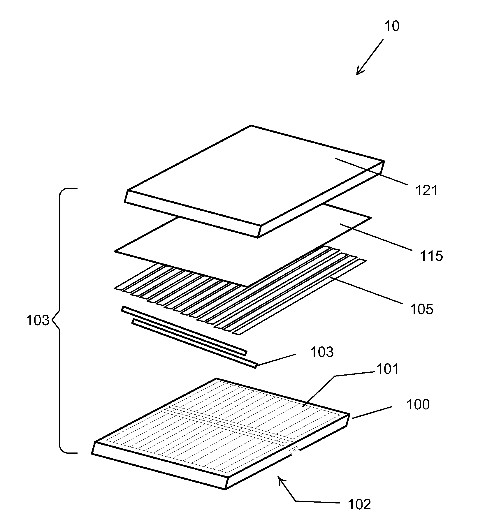
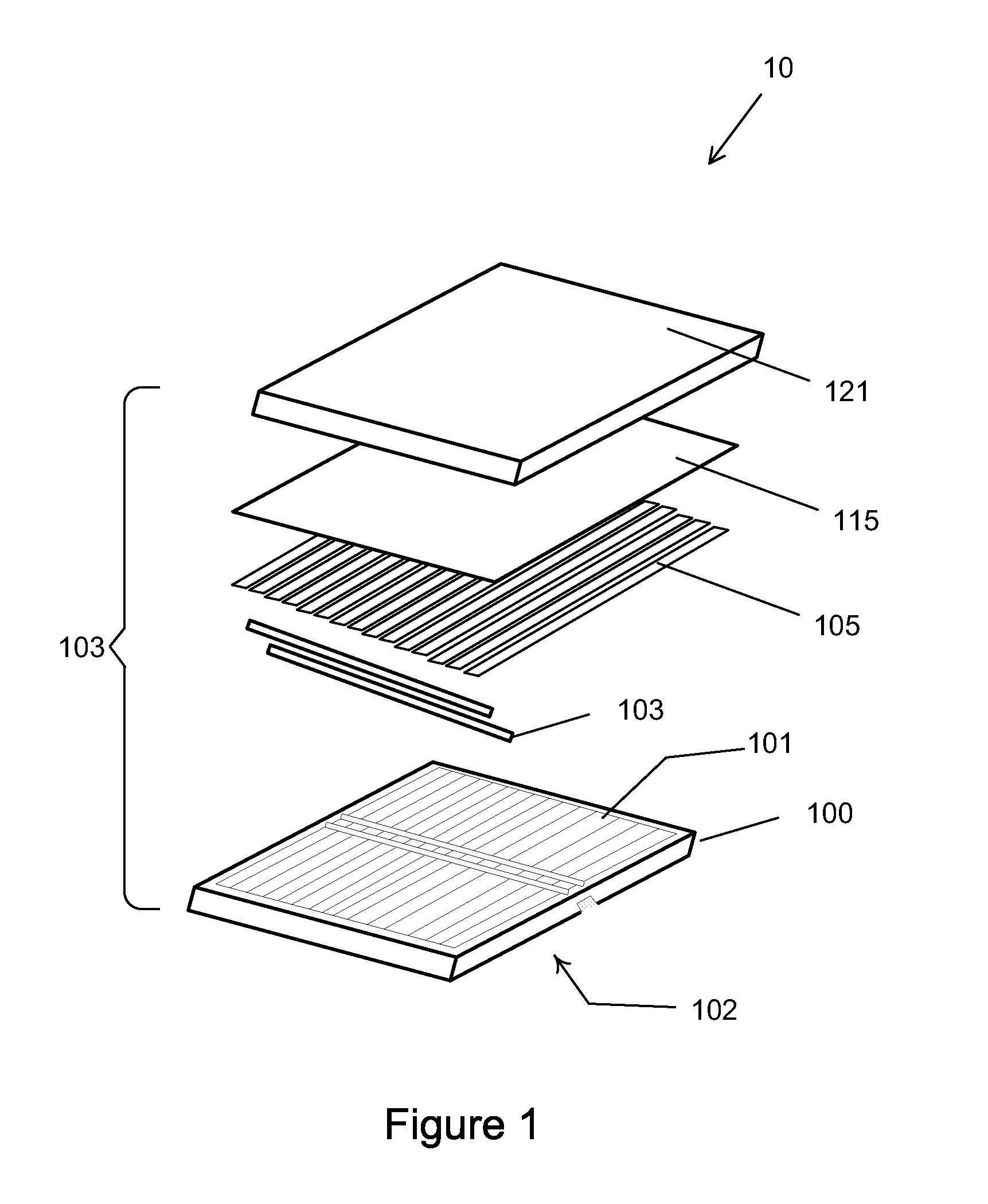
[0023]FIG. 1 is a simplified diagram of a solar cell device 10 according to an embodiment of the present invention. This diagram is merely an example, which should not unduly limit the scope of the claims herein. One of ordinary skill in the art would recognize other variations, modifications, and alternatives. As shown is an expanded view of the present solar cell device structure, which includes various elements. The solar cell device has a back cover member 100, which includes a surface area 101 and a back area 102. The...
PUM
 Abstract
Description
Claims
Application Information