Method and apparatus for improving breakdown voltage of integrated circuits formed using a dielectric layer process

a technology of dielectric layer and breakdown voltage, applied in the field of integrated circuits, can solve the problems of high cost of ic fabrication facilities, difficult devices, electrical failure, etc., and achieve the effects of improving the breakdown voltage of integrated circuits, and being convenient to us

Inactive Publication Date: 2007-06-07
SEMICON MFG INT (SHANGHAI) CORP
View PDF2 Cites 7 Cited by
  • Summary
  • Abstract
  • Description
  • Claims
  • Application Information

AI Technical Summary

Benefits of technology

[0010] Many benefits are achieved by way of the present invention over conventional techniques. For example, the present technique provides an easy to use process that relies upon conventional technology such as silicon materials, although other materials can also be used. Additionally, the method provides a process that is compatible with conventional process technology without substantial modifications to conventional equipment and processes. A method and apparatus for improving the breakdown voltage of integrated circuits formed using a barrier layer process is provided. In a specific embodiment, gas flow bursting that occurs due to residual gas left in gas lines from prior deposition processes is prevented from affecting subsequent deposition process. For example, the breakdown voltage of integrated circuits is improved by at least 75% from wafers when bursting does not occur as compared to wafers where bursting occurred. In another example, reduction in bursting when multiple gas lines are used can be achieved. Depending upon the embodiment, one or more of these benefits may be achieved. These and other benefits will be described in more detail throughout the present specification and more particularly below.

Problems solved by technology

An IC fabrication facility can cost hundreds of millions, or even billions, of dollars.
Making devices smaller is very challenging, as each process used in IC fabrication has a limit.
This can cause electrical failure or impaired performance of the circuit.

Method used


Image

  • Method and apparatus for improving breakdown voltage of integrated circuits formed using a dielectric layer process
  • Method and apparatus for improving breakdown voltage of integrated circuits formed using a dielectric layer process
  • Method and apparatus for improving breakdown voltage of integrated circuits formed using a dielectric layer process

Examples


Embodiment Construction

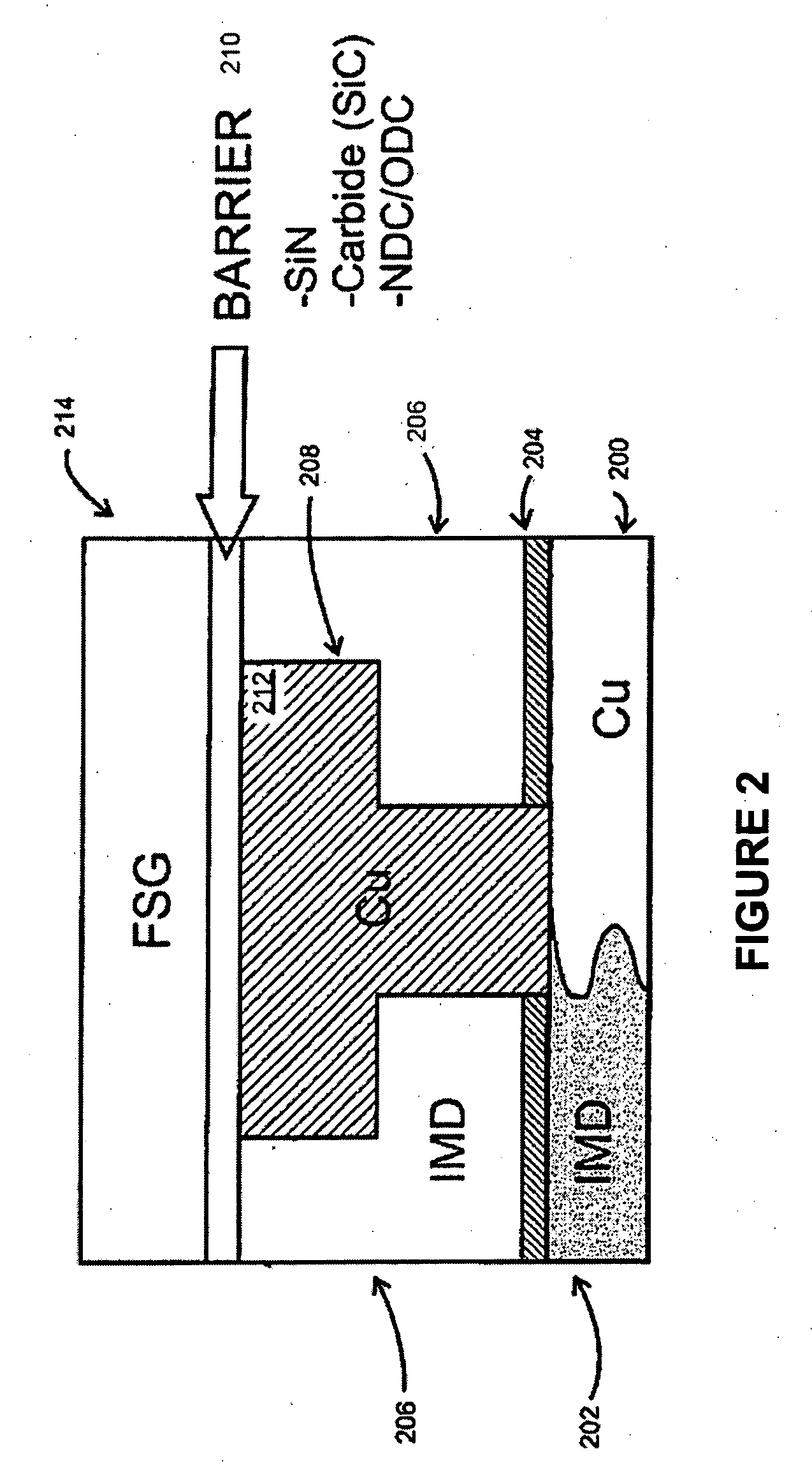
[0024] The present invention is directed to integrated circuits and their processing for the manufacture of semiconductor devices. More particularly, the invention provides a method and apparatus for improving the breakdown voltage of integrated circuits. Merely by way of example, the invention has been applied to a dielectric layer process used in conjunction with a dual damascene structure for signal processing devices. But it would be recognized that the invention has a much broader range of applicability. For example, the invention can be applied to microprocessor devices, logic circuits, application specific integrated circuit devices, as well as various other interconnect structures.

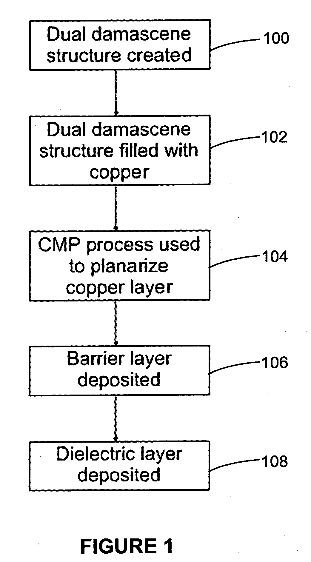
[0025]FIG. 1 is a simplified conventional method showing processes employed during and immediately after a dual damascene process. Method 110 includes a process 100 of creating a dual damascene structure, a process 102 for filling the dual damascene structure with copper, a process 104 for planari...


PUM

PropertyMeasurementUnit
Q-timeaaaaaaaaaa
breakdown voltageaaaaaaaaaa

Abstract

A method and apparatus for depositing a dielectric layer. The apparatus includes a semiconductor processing chamber configured for use in a dielectric layer deposition process, the semiconductor processing chamber being associated with at least a length, a width, a height, and a volume, one or more gas sources containing one or more gases used in the barrier layer deposition process, and one or more gas flow controllers coupled to the one or more gas sources, the one or more gas flow controllers configured to provide one or more controlled amounts of one or more gas flows to the semiconductor processing chamber during semiconductor processing. One or more gas lines coupled to the one or more gas flow controllers for receiving one or more gas flows from the one or more gas flow controllers, and a pumping system is coupled to the semiconductor processing chamber, the pumping system configured to remove a quantity of gas from either the semiconductor processing chamber or the one or more gas lines. A 3-way valve is coupled to the pumping system and the process chamber, the 3-way valve being configured to allow the one or more gas flows to be sent to the pumping system or to the process chamber.

Description

CROSS-REFERENCES TO RELATED APPLICATIONS [0001] This application claims priority to Chinese Patent Application No. 200510111131.8, filed Dec. 5, 2005, commonly assigned and which is incorporated by reference herein for all purposes. BACKGROUND OF THE INVENTION [0002] The present invention is directed to integrated circuits and their processing for the manufacture of semiconductor devices. More particularly, the invention provides a method and apparatus for improving the breakdown voltage of integrated circuits. Merely by way of example, the invention has been applied to a dielectric layer process used in conjunction with a dual damascene structure for signal processing devices. But it would be recognized that the invention has a much broader range of applicability. For example, the invention can be applied to microprocessor devices, logic circuits, application specific integrated circuit devices, as well as various other interconnect structures. [0003] Integrated circuits or “ICs” h...

Claims


Application Information

Patent Timeline
Patent Type & Authority Applications(United States)
IPC IPC(8): H01L21/44C23C16/00
CPCC23C16/4412H01L21/76834
Inventor HOU, KUAN CHENGLAN, SHOU LONGDONG, RUIANG, TING CHEONG
Owner SEMICON MFG INT (SHANGHAI) CORP
Why Eureka
Try Eureka