Method and resulting structure for PCMO film to obtain etching rate and mask to selectively by inductively coupled plasma

a technology of inductively coupled plasma and patterning film, which is applied in the direction of basic electric elements, semiconductor devices, electrical equipment, etc., can solve the problems of limited work performed in cmr materials, small devices are difficult to use, and the etching rate is high, so as to improve etching rate and device yield per wafer. , the effect of improving etching ra

Active Publication Date: 2005-11-24
WINBOND ELECTRONICS CORP
View PDF5 Cites 6 Cited by
  • Summary
  • Abstract
  • Description
  • Claims
  • Application Information

AI Technical Summary

Benefits of technology

[0012] Many benefits are achieved by way of the present invention over conventional techniques. In a specific embodiment, the invention provides a method and system to integrate the CMR materials into the existing conventional semiconductor process technology and fabrication methods without plasma charging damage issues. Additionally, the present technique provides an easy to use process that relies upon conventional technology. In some embodiments, the method provides higher device yields in dies per wafer. Additionally, the method provides a process that is compatible with conventional process technology without substantial modifications to conventional equipment and processes. Preferably, the invention provides for an improved etching technique with higher throughput than conventional technologies. Depending upon the embodiment, one or more of these benefits may be achieved. These and other benefits will be described in more throughout the present specification and more particularly below.

Problems solved by technology

An IC fabrication facility can cost hundreds of millions, or even billions, of dollars.
Making devices smaller is very challenging, as each process used in IC fabrication has a limit.
Unfortunately, limited work has been performed in the CMR materials.
It is considered difficult to etch the thin film of PCMO because of non-volatility of etch byproducts from Pr, Ca, and Mn, and possibly others.
Ion mill can not provide enough mask selectivity which will be a serious concern as the device size continues to shrink beyond 0.13 um technology.

Method used


Image

  • Method and resulting structure for PCMO film to obtain etching rate and mask to selectively by inductively coupled plasma
  • Method and resulting structure for PCMO film to obtain etching rate and mask to selectively by inductively coupled plasma
  • Method and resulting structure for PCMO film to obtain etching rate and mask to selectively by inductively coupled plasma

Examples


Embodiment Construction

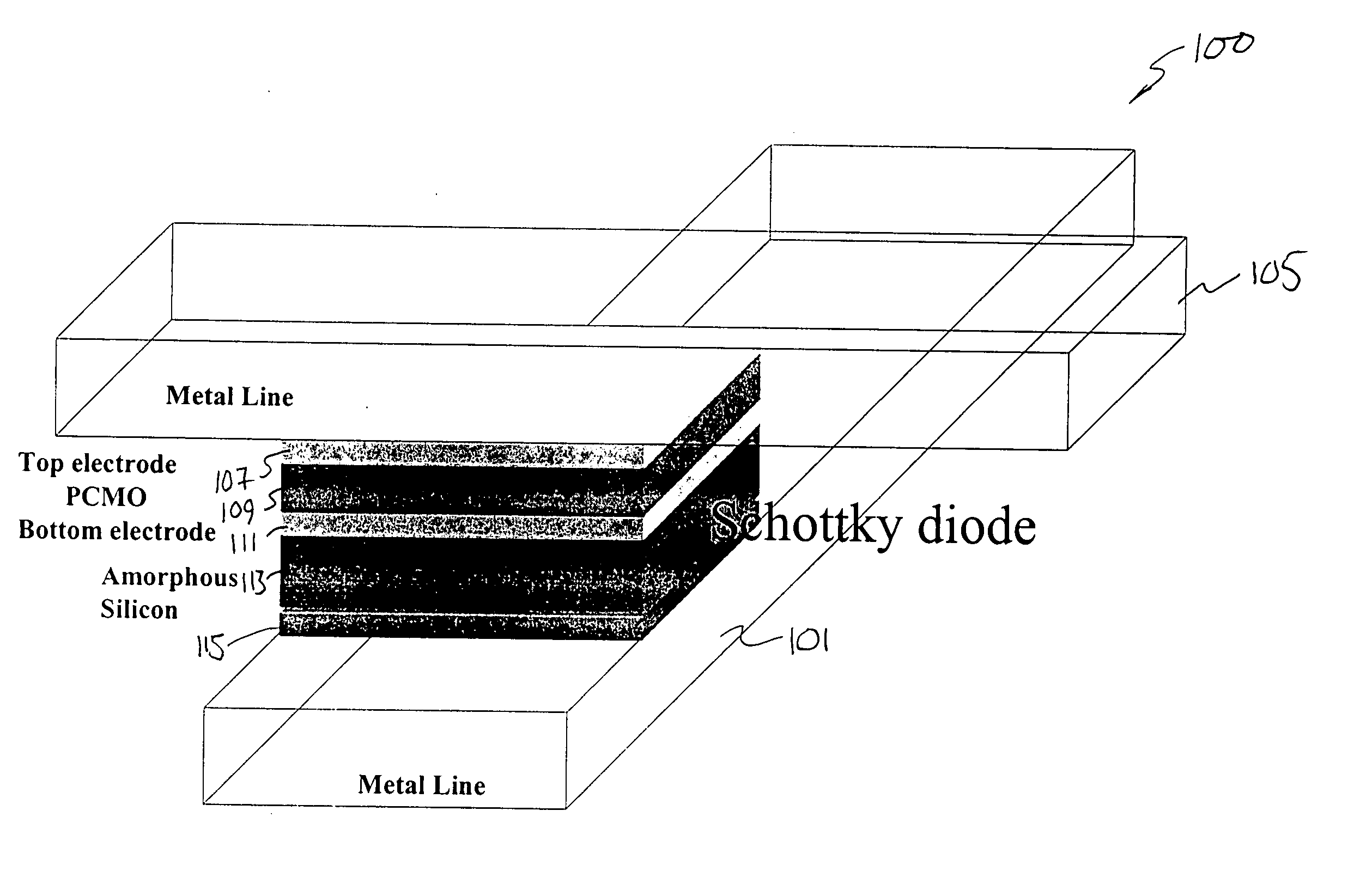
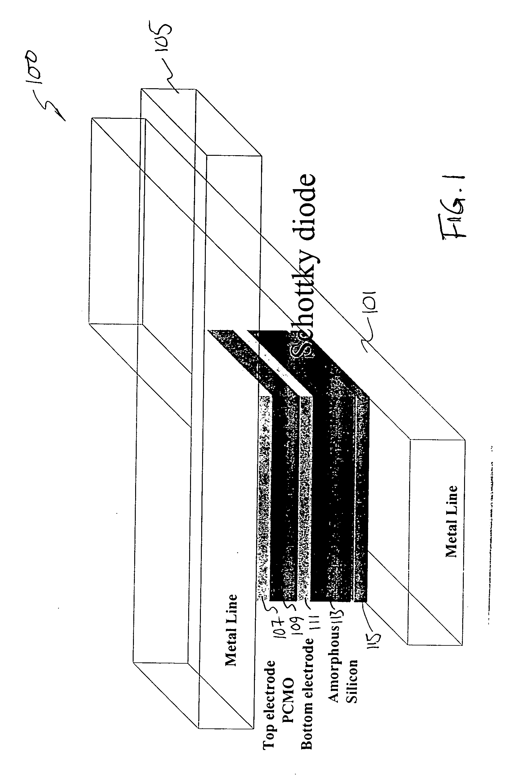
[0020] According to the present invention, techniques directed to integrated circuits and their processing for the manufacture of semiconductor devices are provided. More particularly, the invention provides a method and device for patterning films of PCMO (Pr0.7Ca0.3MnO3) using an etching process. Merely by way of example, the invention has been applied to a resistive material for resistance random access memory (RRAM) devices. But it would be recognized that the invention has a much broader range of applicability. For example, the invention can be applied to microprocessor devices, memory devices, and application specific integrated circuit devices.

[0021]FIG. 1 is a simplified diagram of an RRAM device 100 according to an embodiment of the present invention. This diagram is merely an example, which should not unduly limit the scope of the claims herein. One of ordinary skill in the art would recognize many variations, modifications, and alternatives. As shown, the device includes...


PUM


Abstract

A high selectivity and etch rate with innovative approach of inductively coupled plasma source. Preferably, the invention includes a method using plasma chemistry that is divided into main etch step of (e.g., Cl2+HBr+C4F8) gas combination and over etch step of (e.g., HBr+Ar). The main etch step provides a faster etch rate and selectivity while the over etch step will decrease the etch rate and ensure the stringer and residue removal without attacking the under layer.

Description

BACKGROUND OF THE INVENTION [0001] The present invention is directed to integrated circuits and their processing for the manufacture of semiconductor devices. More particularly, the invention provides a method and device for patterning films of PCMO (Pr0.7Ca0.3MnO3) using an etching process. Merely by way of example, the invention has been applied to a resistive material for resistance random access memory (RRAM) devices. But it would be recognized that the invention has a much broader range of applicability. For example, the invention can be applied to microprocessor devices, memory devices, and application specific integrated circuit devices. [0002] Integrated circuits or “ICs” have evolved from a handful of interconnected devices fabricated on a single chip of silicon to millions of devices. Current ICs provide performance and complexity far beyond what was originally imagined. In order to achieve improvements in complexity and circuit density (i.e., the number of devices capable...

Claims


Application Information

Patent Timeline
Patent Type & Authority Applications(United States)
IPC IPC(8): H01L21/302H01L27/24H01L45/00
CPCH01L45/1625H01L45/1675H01L45/147H01L45/04H01L45/1233H01L27/2409H10B63/20H10N70/20H10N70/8836H10N70/026H10N70/826H10N70/063
Inventor HUANG, KENLINCHOU, K.C.LUAN, HARRYYOUNG, J.C.WANG, ARTHUR
Owner WINBOND ELECTRONICS CORP
Why Eureka
Try Eureka