Projection device provided with semiconductor light source

a technology of light source and projection device, which is applied in the field of system configuration and methods for controlling and operating the projection apparatus, can solve the problems of limited image display quality, adverse effects on image quality, and limitations of high-quality images employed to display high-quality images, so as to reduce the effect of reducing the effect of color break

Inactive Publication Date: 2009-04-23
SILICON QUEST KABUSHIKI KAISHA +1
View PDF30 Cites 18 Cited by
  • Summary
  • Abstract
  • Description
  • Claims
  • Application Information

AI Technical Summary

Benefits of technology

[0028]It is an aspect of the present invention to provide a projection device for displaying images for displaying a higher level of gray scales and higher gradation of resolutions and also reducing the effects of color breaks to an inconspicuous level.
[0057]The twentieth-ninth exemplary embodiment of the present invention is a projection device, comprising a semiconductor light source of different wavelengths, comprising a plurality of sub light sources disposed in an array, an illumination optical system for guiding an illumination light outputted from the semiconductor light source, a spatial light modulator for receiving and applying an image signal for modulating the illumination light outputted from the semiconductor light source guided by said illumination optical system, a control circuit for controlling the semiconductor light source and the spatial light modulator, and a projection optical system for projecting an image by the illumination light modulated by the spatial light modulator, wherein the semiconductor light source has different wavelengths, the control circuit modifies at least one of the following parameters consisted of an emission intensity, a number of times of emission, an emission period and an emitting timing of the sub light source or a number of emitted light and an emitting position of the sub light sources and also controls or adjusts the total length of time of sub-frame time for each wavelength for outputting the illumination light.
[0072]The projection device of the present invention can display an image to be projected by high gradation by controlling or adjusting at least two of the emission intensity, times of emission, emission period and emitting timing of a light source or the number of emitted light and emitting position of a sub light source in synchronization with a spatial light modulator. By appropriately performing such synchronous control or adjustment, color breaks can be made inconspicuous.

Problems solved by technology

Even though there have been significant advances made in recent years in the technologies of implementing electromechanical micromirror devices as spatial light modulators (SLM), there are still limitations and difficulties when they are employed to display high quality images.
Specifically, when the display images are digitally controlled, the quality of the images is adversely affected because the images are not displayed with a sufficient number of gray scale gradations.
The quality of image display is limited due to the limited number of gray scales.
Since the mirror is controlled to operate in either an ON or OFF state, the conventional image display apparatus has no way to provide a pulse width to control the mirror that is shorter than the duration represented by the LSB.
The limited levels of gray scale lead to the degradation of the display image.
In this configuration, reflected light that is not intentionally applied to project an image is, however, inadvertently generated by reflections through the gap between adjacent mirrors.
That leads to the degradations of image quality.
The artifacts are generated by technical limitations in that the digitally controlled image does not provide a sufficient number of the gray scale.
The mirrors produced by applying the CMOS technologies are probably not appropriate for operating the mirror at such a high range of voltages, and therefore DMOS mirror devices may be required.
Conventional mirror controls are therefore faced with a technical problem in that accuracy of gray scales and range of the operable voltage have to be sacrificed for the benefits of a smaller image display apparatus.
However, these patents or patent applications do not provide an effective solution to attain a sufficient number of the gray scale in the digitally controlled image display system.
However, these inventions do not provide a direct solution for a person skilled in the art to overcome the above-discussed limitations and difficulties.

Method used


Image

  • Projection device provided with semiconductor light source
  • Projection device provided with semiconductor light source
  • Projection device provided with semiconductor light source

Examples


Embodiment Construction

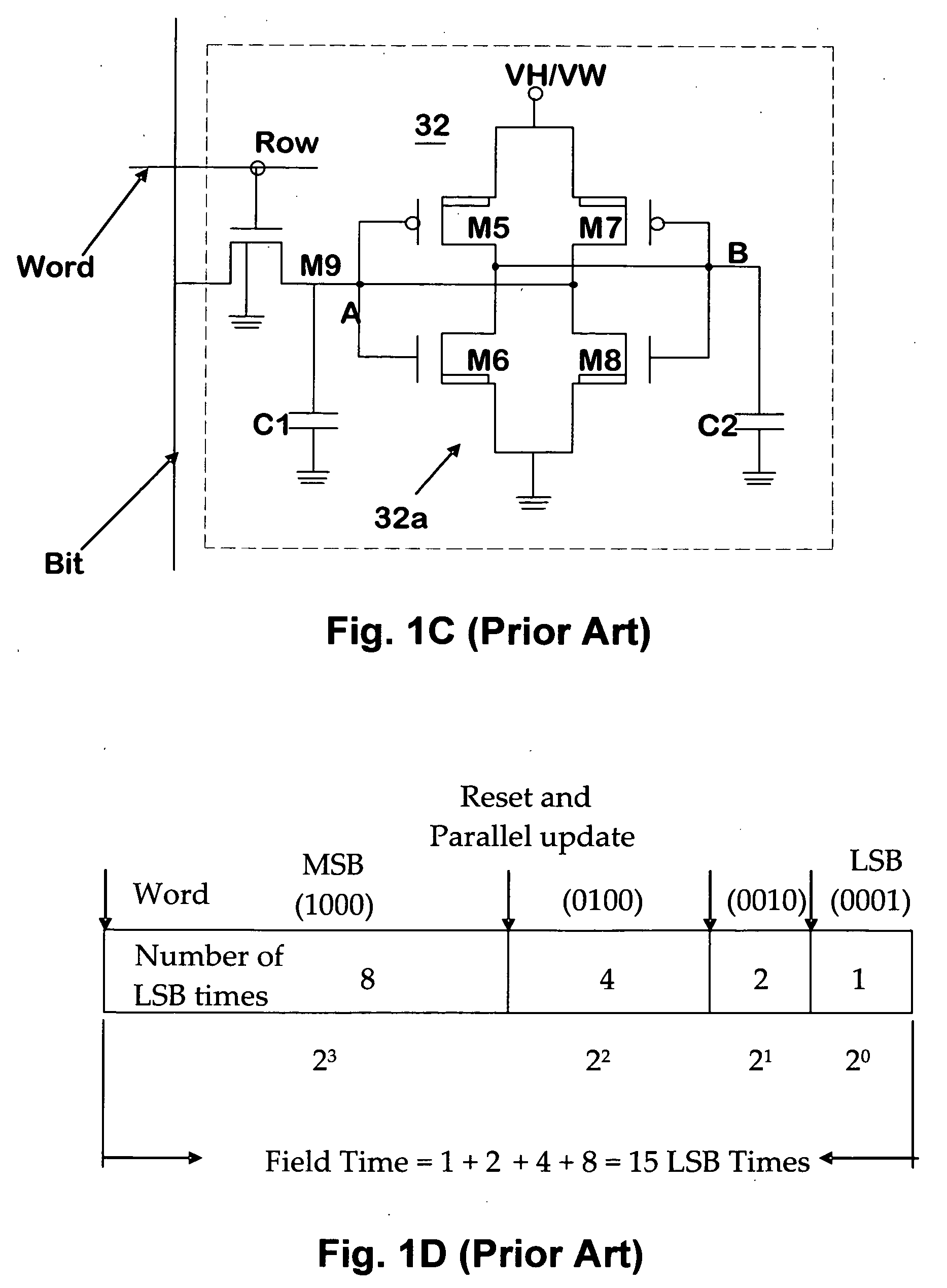
[0121]First, the method of specifying the deflection angles of a deflectable mirror in a mirror device in this preferred embodiment is briefly described.

[Summary of Device]

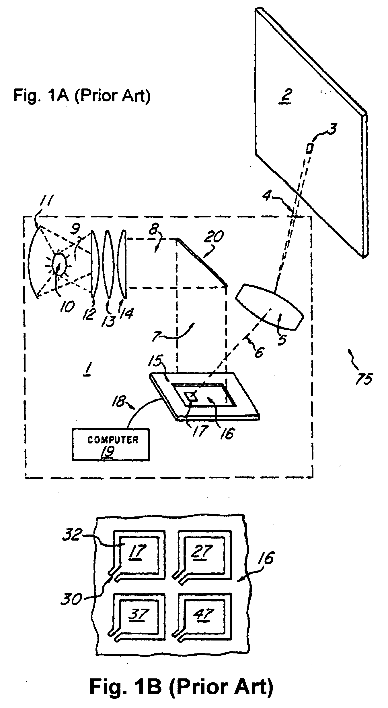
[0122]Projection apparatuses using a spatial light modulator, such as a transmissive liquid crystal, a reflective liquid crystal, a mirror array, etc., are widely known.

[0123]A spatial light modulator includes a two-dimensional array that arranges, enlarges, and then displays onto a screen by way of a projection lens arrayed as tens of thousands to millions of miniature modulation elements for projecting individual pixels corresponding to an image.

[0124]The spatial light modulators generally used for projection apparatuses are of primarily two types: 1) a liquid crystal device for modulating the polarizing direction of incident light; a liquid crystal is sealed between transparent substrates and provides them with a potential, and 2) a mirror device that deflects miniature micro electro mechanical systems (MEMS) m...


PUM


Abstract

The present invention provides a projection device comprising a semiconductor light source comprises a plurality of sub light sources arranged in an array, an illumination optical system for guiding an illumination light emitted from the semiconductor light source, a spatial light modulator for receiving and applying an image signal for modulating the illumination light emitted from the semiconductor light source guided by said illumination optical system, a control circuit for controlling the semiconductor light source and the spatial light modulator and a projection optical system for projecting images by applying the illumination light modulated by the spatial light modulator. The control circuit controls or adjusts the emitting state of the semiconductor light source by modifying at least two of following parameters consisted of an emission intensity, a number of times of emission, an emission period and an emitting timing of the sub light source or a number of emitted light and an emitting position of the sub light sources.

Description

CROSS REFERENCE TO RELATED APPLICATIONS[0001]This application is a Non-provisional Application claiming a Priority date of Oct. 2, 2007 based on a previously filed Provisional Application 60 / 997,728 and a Non-provisional patent application Ser. No. 11 / 121,543 filed on May 3, 2005 issued into U.S. Pat. No. 7,268,932. The application Ser. No. 11 / 121,543 is a Continuation In Part (CIP) Application of three previously filed Applications. These three Applications are Ser. No. 10 / 698,620 filed on Nov. 1, 2003, Ser. No. 10 / 699,140 filed on Nov. 1, 2003 now issued into U.S. Pat. No. 6,862,127, and Ser. No. 10 / 699,143 filed on Nov. 1, 2003 now issued into U.S. Pat. No. 6,903,860 by the Applicant of this Patent Applications. The disclosures made in these Patent Applications are hereby incorporated by reference in this Patent Application.BACKGROUND OF THE INVENTION[0002]1. Field of the Invention[0003]The present invention relates generally to the field of system configuration and methods for c...

Claims


Application Information

Patent Timeline
Patent Type & Authority Applications(United States)
IPC IPC(8): H04N5/74
CPCG03B21/2013G03B21/2033H04N9/3155G03B33/06H04N9/3123G03B21/2053
Inventor MAEDA, YOSHIHIROARAI, KAZUMAENDO, TAROISHII, FUSAO
Owner SILICON QUEST KABUSHIKI KAISHA
Why Eureka
Try Eureka