

Organic light emitting diode display and method for manufacturing the same
a light-emitting diode and display technology, applied in semiconductor devices, instruments, electrical devices, etc., can solve the problems of narrow viewing angle, difficult to minutely form the edge portions of the opening, slow response time, etc., and achieve the effect of increasing the aperture ratio
- Summary
- Abstract
- Description
- Claims
- Application Information
AI Technical Summary
Benefits of technology
Problems solved by technology
Method used
Image

Examples
first embodiment
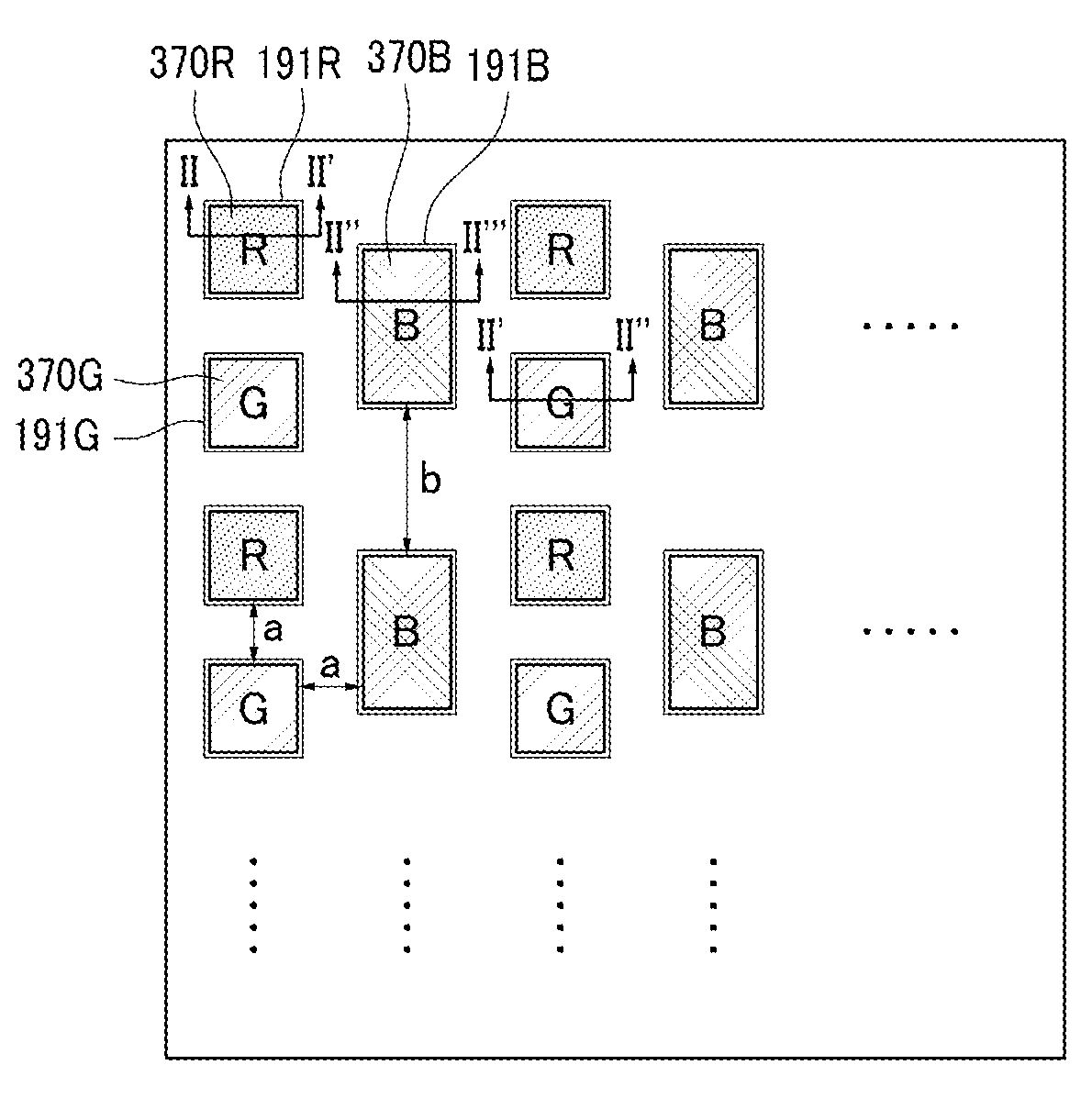
[0045]An organic light emitting device according to an exemplary embodiment of the present invention will be described in detail with reference to FIG. 1 and FIG. 2.
[0046]FIG. 1 is a top plan view schematically showing the arrangement of a plurality of pixels in an organic light emitting device according to an exemplary embodiment of the present invention, and FIG. 2 is a cross-sectional view taken along lines II-II′, II′-II″, and II″-II′″ of FIG. 1.
[0047]Referring to FIG. 1, an organic light emitting device according to an exemplary embodiment of the present invention includes red pixels R to display a red color, green pixels G to display a green color, and blue pixels B to display a blue color. The red pixels R, the green pixels G, and the blue pixels B form the basic pixel, which is used to display full colors, and three pixels forming one group are repeated according to a row and column.
[0048]In detail, the plurality of red pixels R and the plurality of green pixels G are altern...
second embodiment
[0079]An organic light emitting device according to another exemplary embodiment of the present invention will be described in detail below with reference to FIG. 10 and FIG. 11.
[0080]FIG. 10 is a top plan view schematically showing the arrangement of a plurality of pixels in an organic light emitting device according to the present exemplary embodiment of the present invention, and FIG. 11 is a cross-sectional view schematically showing a red pixel R, a green pixel G, and a blue pixel B taken along lines XI-XI′, XI′-XI″, and XI″-XI′″ shown in FIG. 10.
[0081]Referring to FIG. 10, regarding the arrangement of the pixels in an organic light emitting device according to this exemplary embodiment, the plurality of red pixels R and the plurality of green pixels G are alternately arranged in a first column, and the plurality of blue pixels B are continuously arranged in a second column, like the above-described embodiment.
[0082]Also, the red pixels R and the blue pixels B are alternately a...
third embodiment
[0098]An organic light emitting device according to another exemplary embodiment of the present invention will be described in detail below with reference to FIG. 14 and FIG. 15.
[0099]FIG. 14 is a top plan view schematically showing the arrangement of a plurality of pixels in an organic light emitting device according to another exemplary embodiment of the present invention, and FIG. 15 is a cross-sectional view schematically showing a red pixel R, a green pixel G, and a blue pixel B taken along lines XV-XV′ and XV′-XV″ shown in FIG. 14.
[0100]Referring to FIG. 14, the plurality of red pixels R and the plurality of blue pixels B are alternately arranged in a row, and the plurality of green pixels G and the plurality of blue pixels B are also alternately arranged in a row, like the above-described embodiment.
[0101]Here, the intervals g between the red pixels R and the green pixels G, between the red pixels R and the blue pixels B, and between the green pixels G and the blue pixels B a...
PUM
 Abstract
Description
Claims
Application Information